SLVSB16E November 2011 – December 2015 TPS43340-Q1
PRODUCTION DATA.
- 1 Features
- 2 Applications
- 3 Description
- 4 Revision History
- 5 Pin Configuration and Functions
- 6 Specifications
-
7 Detailed Description
- 7.1 Overview
- 7.2 Functional Block Diagram
- 7.3 Feature Description
- 7.4 Device Functional Modes
- 8 Application and Implementation
- 9 Power Supply Recommendations
- 10Layout
- 11Device and Documentation Support
- 12Mechanical, Packaging, and Orderable Information
1 Features
- Qualified for Automotive Applications
- AEC-Q100 Test Guidance With the Following Results:
- Device Temperature Grade 1: –40°C to 125°C Ambient Operating Temperature
- Device HBM ESD Classification Level H1C
- Device CDM ESD Classification Level C3B
- Input Range up to 40 V, (Transients up to 60 V)
- Input Voltage Range: 4 V to 40 V
- Transients up to 60 V
- Dual-Output Synchronous Buck Controller
- Peak Gate Drive Current 0.6 A
- Automatic Low-Power Mode Operation
- Low-Power-Mode IQ : 30 µA (One Buck On), 35 µA (Two Bucks On)
- Low Shutdown Current, Ish = 5 μA Typical
- Single Synchronous Buck Regulator Converter BUCK3
- Max Output Current 2 A
- Linear Regulator LREG1
- Separate Enable Inputs (EN1, EN2, EN3, EN4)
- Internal Oscillator, Programmable via External Resistor, 150 kHz to 600 kHz for Switching Frequency fSW_BUCK1,2,3
- Integrated PLL, External Synchronization Frequency: 150 kHz to 600 kHz
- Switch-Mode Regulators Operate With 180° Phase-Shift
- Reset Output for All Output Rails
- Supply and Overvoltage Detection and Shutdown
- Thermally Enhanced PowerPAD™ Package
- 48-Pin HTQFP (PHP)
2 Applications
- Automotive Infotainment, Head Unit, Navigation, Audio and Clusters
- Advanced Driver Assistance System (ADAS)
- Automotive and Industrial Multi-Rail DC Power Distribution Systems
3 Description
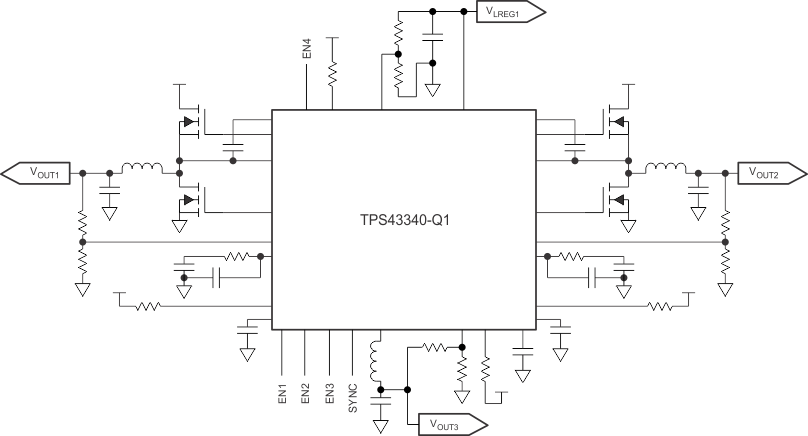
The TPS43340-Q1 is a quad rail power supply featuring two synchronous Buck Controller with 0.6-A gate drive, one synchronous 2-A Buck Converter and a 300-mA LDO with low quiescent current. The device is designed to power the entire system including MCU and DSP straight from the car battery respectively input voltages up to 40 V. The device features integrated short-circuit and overcurrent protection on the gate-drive outputs for the buck regulator controllers and independent current-foldback control for each buck regulator supply during regulator output short to ground. Each output supply incorporates a soft start to ensure that on initial power up these regulated outputs are not in current limit. Implementation of reset delay on power up allows the outputs of Buck1, Buck2, Buck3 and the linear regulator to get to stable regulation. An external capacitor sets the delay to a maximum range of 300 ms. Each power-supply output has adjustable output voltage based on the external resistor-network settings. The device has sequencing control during power up and power down of the output rails, based on the enable-and-disable control or soft start.
Device Information(1)
| PART NUMBER | PACKAGE | BODY SIZE (NOM) |
|---|---|---|
| TPS43340-Q1 | HTQFP (48) | 7.00 mm × 7.00 mm |
- For all available packages, see the orderable addendum at the end of the data sheet.
