SLVSB69C June 2012 – September 2021 TPS54719
PRODUCTION DATA
- 1 Features
- 2 Applications
- 3 Description
- 4 Revision History
- 5 Pin Configuration and Functions
- 6 Specifications
-
7 Detailed Description
- 7.1 Overview
- 7.2 Functional Block Diagram
- 7.3
Feature Description
- 7.3.1 Fixed Frequency PWM Control
- 7.3.2 Slope Compensation And Output Current
- 7.3.3 Bootstrap Voltage (Boot) And Low Dropout Operation
- 7.3.4 Error Amplifier
- 7.3.5 Voltage Reference
- 7.3.6 Adjusting The Output Voltage
- 7.3.7 Enable and Adjusting Undervoltage Lockout
- 7.3.8 Slow Start/Tracking Pin
- 7.3.9 Sequencing
- 7.4
Device Functional Modes
- 7.4.1 Constant Switching Frequency And Timing Resistor (RT Pin)
- 7.4.2 Overcurrent Protection
- 7.4.3 Frequency Shift
- 7.4.4 Reverse Overcurrent Protection
- 7.4.5 Power Good (PWRGD Pin)
- 7.4.6 Overvoltage Transient Protection
- 7.4.7 Thermal Shutdown
- 7.4.8 Small Signal Model For Loop Response
- 7.4.9 Simple Small Signal Model For Peak Current Mode Control
- 7.4.10 Small Signal Model For Frequency Compensation
-
8 Application and Implementation
- 8.1 Application Information
- 8.2
Typical Application
- 8.2.1 High Frequency, 1.8-V Output Power Supply Design With Adjusted UVLO
- 8.2.2 Design Requirements
- 8.2.3
Detailed Design Procedure
- 8.2.3.1 Selecting The Switching Frequency
- 8.2.3.2 Output Inductor Selection
- 8.2.3.3 Output Capacitor
- 8.2.3.4 Input Capacitor
- 8.2.3.5 Slow-Start Capacitor
- 8.2.3.6 Bootstrap Capacitor Selection
- 8.2.3.7 Undervoltage Lockout Set Point
- 8.2.3.8 Output Voltage And Feedback Resistors Selection
- 8.2.3.9 Compensation
- 8.2.4 Application Curves
- 9 Power Supply Recommendations
- 10Layout
- 11Device and Documentation Support
- 12Mechanical, Packaging, and Orderable Information
10.2.1 Power Dissipation Estimate
The following formulas show how to estimate the IC power dissipation under continuous conduction mode (CCM) operation. The power dissipation of the IC (Ptot) includes the following:
- Conduction loss (Pcon)
- Dead time loss (Pd)
- Switching loss (Psw)
- Gate drive loss (Pgd)
- Supply current loss (Pq)
Pcon = Io2 × Rdson_temp
Pd = ƒsw × Iout × 0.7 × 70 × 10-9
Psw = 0.5 × Vin × Io × ƒsw × 9 × 10⁻⁹
Pgd = 2 × Vin × 6 × 10⁻⁹ × ƒsw
Pq = 455 × 10-6 × Vin
where:
- IOUT is the output current (A)
- Rdson is the on-resistance of the high-side MOSFET (Ω)
- VIN is the input voltage (V)
- ƒsw is the switching frequency (Hz)
So
Ptot = Pcon + Pd + Psw + Pgd + Pq
For given TA,
TJ = TA + Rth × Ptot
For given TJMAX = 140°C
TAmax = TJMAX – Rth × Ptot
where:
- Ptot is the total device power dissipation (W)
- TA is the ambient temperature (°C)
- TJ is the junction temperature (°C)
- Rth is the thermal resistance of the package (°C/W)
- TJMAX is maximum junction temperature (°C)
- TAMAX is maximum ambient temperature (°C)
There are additional power losses in the regulator circuit due to the inductor AC and DC losses and trace resistance that impact the overall efficiency of the regulator.
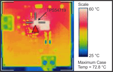
 Figure 10-2 Thermal
Image, IOUT = 7 A