SLVSB69C June 2012 – September 2021 TPS54719
PRODUCTION DATA
- 1 Features
- 2 Applications
- 3 Description
- 4 Revision History
- 5 Pin Configuration and Functions
- 6 Specifications
-
7 Detailed Description
- 7.1 Overview
- 7.2 Functional Block Diagram
- 7.3
Feature Description
- 7.3.1 Fixed Frequency PWM Control
- 7.3.2 Slope Compensation And Output Current
- 7.3.3 Bootstrap Voltage (Boot) And Low Dropout Operation
- 7.3.4 Error Amplifier
- 7.3.5 Voltage Reference
- 7.3.6 Adjusting The Output Voltage
- 7.3.7 Enable and Adjusting Undervoltage Lockout
- 7.3.8 Slow Start/Tracking Pin
- 7.3.9 Sequencing
- 7.4
Device Functional Modes
- 7.4.1 Constant Switching Frequency And Timing Resistor (RT Pin)
- 7.4.2 Overcurrent Protection
- 7.4.3 Frequency Shift
- 7.4.4 Reverse Overcurrent Protection
- 7.4.5 Power Good (PWRGD Pin)
- 7.4.6 Overvoltage Transient Protection
- 7.4.7 Thermal Shutdown
- 7.4.8 Small Signal Model For Loop Response
- 7.4.9 Simple Small Signal Model For Peak Current Mode Control
- 7.4.10 Small Signal Model For Frequency Compensation
-
8 Application and Implementation
- 8.1 Application Information
- 8.2
Typical Application
- 8.2.1 High Frequency, 1.8-V Output Power Supply Design With Adjusted UVLO
- 8.2.2 Design Requirements
- 8.2.3
Detailed Design Procedure
- 8.2.3.1 Selecting The Switching Frequency
- 8.2.3.2 Output Inductor Selection
- 8.2.3.3 Output Capacitor
- 8.2.3.4 Input Capacitor
- 8.2.3.5 Slow-Start Capacitor
- 8.2.3.6 Bootstrap Capacitor Selection
- 8.2.3.7 Undervoltage Lockout Set Point
- 8.2.3.8 Output Voltage And Feedback Resistors Selection
- 8.2.3.9 Compensation
- 8.2.4 Application Curves
- 9 Power Supply Recommendations
- 10Layout
- 11Device and Documentation Support
- 12Mechanical, Packaging, and Orderable Information
3 Description
The TPS54719 device is a full featured 6-V, 7-A, synchronous step down current mode converter with two integrated MOSFETs.
The TPS54719 enables small designs by integrating the MOSFETs, implementing current mode control to reduce external component count, reducing inductor size by enabling up to 2-MHz switching frequency, and minimizing the IC footprint with a small 3-mm × 3-mm thermally enhanced QFN package.
The TPS54719 provides accurate regulation for a variety of loads with an accurate ±1.5% Voltage Reference (VREF) over temperature.
Efficiency is maximized through the integrated 30-mΩ MOSFETs and 455-μA typical supply current. Using the enable pin, shutdown supply current is reduced to 1 μA by entering a shutdown mode.
Undervoltage lockout is internally set at 2.4 V, but can be increased by programming the threshold with a resistor network on the enable pin. The output voltage start-up ramp is controlled by the slow-start pin. An open-drain power-good signal indicates the output is within 93% to 108% of its nominal voltage.
Frequency foldback and thermal shutdown protects the device during an overcurrent condition.
The TPS54719 is supported in the WEBENCH™ Software Tool at www.ti.com/webench.
| PART NUMBER | PACKAGE(1) | BODY SIZE (NOM) |
|---|---|---|
| TPS54719 | QFN (16) | 3.00 mm × 3.00 mm |
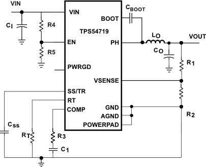
 Simplified Schematic
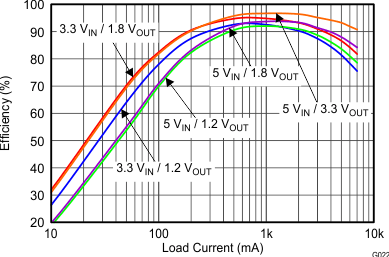
 Efficiency Versus Output
Current