SLVSB70C October 2013 – January 2021 TPS62085 , TPS62086 , TPS62087
PRODUCTION DATA
- 1 Features
- 2 Applications
- 3 Description
- 4 Revision History
- 5 Device Options
- 6 Pin Configuration and Functions
- 7 Specifications
- 8 Detailed Description
- 9 Application and Implementation
- 10Power Supply Recommendations
- 11Layout
- 12Device and Documentation Support
9.2.3 Application Curves
VIN = 3.6 V, VOUT = 1.2 V, TA = 25°C, unless otherwise noted
Table 9-5 Table of Graphs
| FIGURE | ||
|---|---|---|
| Efficiency | TPS62085, VOUT = 0.95 V | Figure 9-2 |
| TPS62085, VOUT = 1.2 V | Figure 9-3 | |
| TPS62086, VOUT = 3.3 V | Figure 9-4 | |
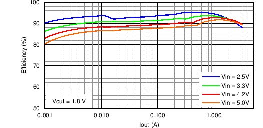
| TPS62087, VOUT = 1.8 V | Figure 9-5 | |
| Line Regulation | TPS62085 | Figure 9-6 |
| Load Regulation | TPS62085 | Figure 9-7 |
| Switching Frequency | TPS62085 | Figure 7-1 |
| Waveforms | TPS62085, PWM Operation (Load = 3 A) | Figure 9-8 |
| TPS62085, PSM Operation (Load = 100 mA) | Figure 9-9 | |
| TPS62085, Load Sweep (Load = Open to 3 A) | Figure 9-10 | |
| TPS62085, Start-Up (Load = 0.47 Ω) | Figure 9-11 | |
| TPS62085, Start-Up (Load = Open) | Figure 9-12 | |
| TPS62085, Shutdown (Load = 0.47 Ω) | Figure 9-13 | |
| TPS62085, Shutdown (Load = Open) | Figure 9-14 | |
| TPS62085, Load Transient (Load = 0.5 A to 3 A) | Figure 9-15 | |
| TPS62085, Load Transient (Load = 50 mA to 3 A) | Figure 9-16 | |
| TPS62085, Output Short-Circuit Protection (Load = 0.47 Ω, Entry) | Figure 9-17 | |
| TPS62085, Output Short-Circuit Protection (Load = 0.47 Ω, Recovery) | Figure 9-18 | |
| TPS62085, Output Short-Circuit Protection (Load = 0.47 Ω, HICCUP Zoom In) | Figure 9-19 | |
 Figure 9-2 Efficiency
 Figure 9-4 Efficiency
 Figure 9-6 Line Regulation
 Figure 9-8 PWM Operation, Load = 3 A
 Figure 9-10 Load Sweep, Load = Open to 3 A
 Figure 9-12 Start-Up, Load = Open
 Figure 9-14 Shutdown, Load = Open
 Figure 9-16 Load Transient, Load = 50 mA to 3 A
 Figure 9-18 Output Short-Circuit Protection, Load = 0.47 Ω, Recovery
 Figure 9-3 Efficiency
 Figure 9-5 Efficiency
 Figure 9-7 Load Regulation
 Figure 9-9 PSM Operation, Load = 100 mA
 Figure 9-11 Start-Up, Load = 0.47 Ω
 Figure 9-13 Shutdown, Load = 0.47 Ω
 Figure 9-15 Load Transient, Load = 0.5 A to 3 A
 Figure 9-17 Output Short-Circuit Protection, Load = 0.47 Ω, Entry
 Figure 9-19 Output Short-Circuit Protection, Load = 0.47 Ω, HICCUP Zoom In