SLVSB97E July 2012 – January 2018 TPS23751 , TPS23752
PRODUCTION DATA.
- 1 Features
- 2 Applications
- 3 Description
- 4 Revision History
- 5 Pin Configuration and Functions
-
6 Specifications
- 6.1 Absolute Maximum Ratings
- 6.2 ESD Ratings
- 6.3 ESD Ratings: Surge
- 6.4 Recommended Operating Conditions
- 6.5 Thermal Information
- 6.6 Electric Characteristics - Controller Section
- 6.7 Electrical Characteristics - Sleep Mode (TPS23752 Only)
- 6.8 Electrical Characteristics - PoE Interface Section
- 6.9 Typical Characteristics
-
7 Detailed Description
- 7.1 Overview
- 7.2 Functional Block Diagrams
- 7.3 Feature Description
- 7.4
Device Functional Modes
- 7.4.1 PoE Overview
- 7.4.2
Sleep Mode Operation (TPS23752 only)
- 7.4.2.1 Converter Controller Features
- 7.4.2.2 PWM and VFO Operation; CTL, SRT, and SRD Pin Relationships to Output Load Current
- 7.4.2.3 Bootstrap Topology
- 7.4.2.4 Current Slope Compensation and Current Limit
- 7.4.2.5 RT
- 7.4.2.6 T2P, Startup and Power Management
- 7.4.2.7 Thermal Shutdown
- 7.4.2.8 Adapter ORing
- 7.4.2.9 Using DEN to Disable PoE
- 7.4.2.10 ORing Challenges
-
8 Application and Implementation
- 8.1 Application Information
- 8.2
Typical Application
- 8.2.1 Design Requirements
- 8.2.2
Detailed Design Procedure
- 8.2.2.1 Input Bridges and Schottky Diodes
- 8.2.2.2 Protection, D1
- 8.2.2.3 Capacitor, C1
- 8.2.2.4 Detection Resistor, RDEN
- 8.2.2.5 Classification Resistor, RCLS
- 8.2.2.6 APD Pin Divider Network, RAPD1, RAPD2
- 8.2.2.7 Setting the PWM-VFO Threshold using the SRT pin
- 8.2.2.8 Setting Frequency (RT)
- 8.2.2.9 Current Slope Compensation
- 8.2.2.10 Voltage Feed-Forward Compensation
- 8.2.2.11 Estimating Bias Supply Requirements and Cvc
- 8.2.2.12 Switching Transformer Considerations and RVC
- 8.2.2.13 T2P Pin Interface
- 8.2.2.14 Softstart
- 8.2.2.15 Special Switching MOSFET Considerations
- 8.2.2.16 ESD
- 8.2.2.17 Thermal Considerations and OTSD
- 8.2.3 Application Curves
- 9 Power Supply Recommendations
- 10Layout
- 11Device and Documentation Support
- 12Mechanical, Packaging, and Orderable Information
7.4.2.8 Adapter ORing
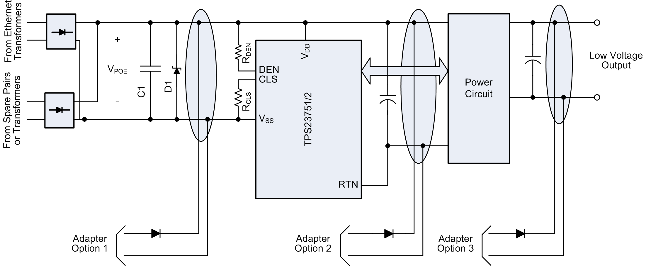
Many PoE-capable devices are designed to operate from either a wall adapter or PoE power. A local power solution adds cost and complexity, but allows a product to be used if PoE is not available in a particular installation. While most applications only require that the PD operate when both sources are present, the TPS23751 and TPS23752 supports forced operation from either of the power sources. Figure 30 illustrates three options for diode ORing external power into a PD. Only one option would be used in any particular design. Option 1 applies power to the TPS23751 and TPS23752 PoE input, option 2 applies power between the TPS23751 and TPS23752 PoE section and the power circuit, and option 3 applies power to the output side of the converter. Each of these options has advantages and disadvantages. Many of the basic ORing configurations and much of the discussion contained in the application note Advanced Adapter ORing Solutions using the TPS23753 (SLVA306), apply to the TPS23751 and TPS23752.
 Figure 30. ORing Configurations
The IEEE standards require that the Ethernet cable be isolated from ground and all other system potentials. The adapter must meet a minimum 1500 Vac dielectric withstand test between the output and all other connections for ORing options 1 and 2. The adapter only needs this isolation for option 3 if it is not provided by the converter.
Adapter ORing diodes are shown for all the options to protect against a reverse voltage adapter, a short on the adapter input pins, or damage to a low-voltage adapter. ORing is sometimes accomplished with a MOSFET in option 3.