SLVSCO0E June 2014 – October 2020 TPS22914 , TPS22915
PRODUCTION DATA
- 1 Features
- 2 Applications
- 3 Description
- 4 Revision History
- 5 Device Comparison Table
- 6 Pin Configuration and Functions
- 7 Specifications
- 8 Parameter Measurement Information
- 9 Detailed Description
- 10Application and Implementation
- 11Power Supply Recommendations
- 12Layout
- 13Device and Documentation Support
- 14Mechanical, Packaging, and Orderable Information
3 Description
The TPS22914/15 is a small, low RON, single channel load switch with controlled slew rate. The device contains an N-channel MOSFET that can operate over an input voltage range of 1.05 V to 5.5 V and can support a maximum continuous current of 2 A. The switch is controlled by an on and off input, which is capable of interfacing directly with low-voltage control signals.
The small size and low RON makes the device ideal for being used in space constrained, battery powered applications. The wide input voltage range of the switch makes it a versatile solution for many different voltage rails. The controlled rise time of the device greatly reduces inrush current caused by large bulk load capacitances, thereby reducing or eliminating power supply droop. The TPS22915 further reduces the total solution size by integrating a 143-Ω pull-down resistor for quick output discharge (QOD) when the switch is turned off.
The TPS22914/15 is available in a small, space-saving 0.78 mm x 0.78 mm, 0.4-mm pitch, 0.5-mm height 4-pin Wafer-Chip-Scale (WCSP) package (YFP). The device is characterized for operation over the free-air temperature range of –40°C to +105°C.
| PART NUMBER | PACKAGE | BODY SIZE (NOM) |
|---|---|---|
| TPS22914B | DSBGA (4) | 0.74 mm x 0.74 mm |
| TPS22914C | ||
| TPS22915B | ||
| TPS22915C |
 Simplified Schematic
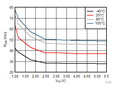
 RON vs VIN
(IOUT = –200 mA)