SLVSD94F
November 2017 – November 2024
TPS62088
,
TPS62088A
,
TPS62089A
PRODUCTION DATA
1
1
Features
2
Applications
3
Description
4
Device Options
5
Pin Configuration and Functions
6
Specifications
6.1
Absolute Maximum Ratings
6.2
ESD Ratings
6.3
Recommended Operating Conditions
6.4
Thermal Information
6.5
Electrical Characteristics
6.6
Typical Characteristics
7
Detailed Description
7.1
Overview
7.2
Functional Block Diagram
7.3
Feature Description
7.3.1
Power Save Mode
7.3.2
Pulse Width Modulation (PWM) Operation
7.3.3
100% Duty Cycle Low Dropout Operation
7.3.4
Soft Start
7.3.5
Switch Current Limit and HICCUP Short-Circuit Protection
7.3.6
Undervoltage Lockout
7.3.7
Thermal Shutdown
7.4
Device Functional Modes
7.4.1
Enable and Disable
7.4.2
Power Good
8
Application and Implementation
8.1
Application Information
8.2
Typical Application
8.2.1
Design Requirements
8.2.2
Detailed Design Procedure
8.2.2.1
Custom Design With WEBENCH® Tools
8.2.2.2
Setting The Output Voltage
8.2.2.3
Feedforward Capacitor
8.2.2.4
Output Filter Design
8.2.2.5
Inductor Selection
8.2.2.6
Capacitor Selection
8.2.3
Application Curves
8.3
Power Supply Recommendations
8.4
Layout
8.4.1
Layout Guidelines
8.4.2
Layout Example
8.4.2.1
Thermal Considerations
9
Device and Documentation Support
9.1
Device Support
9.1.1
Third-Party Products Disclaimer
9.1.2
Development Support
9.1.2.1
Custom Design With WEBENCH® Tools
9.2
Documentation Support
9.2.1
Related Documentation
9.3
Receiving Notification of Documentation Updates
9.4
Support Resources
9.5
Trademarks
9.6
Electrostatic Discharge Caution
9.7
Glossary
10
Revision History
11
Mechanical, Packaging, and Orderable Information
8.4.2
Layout Example
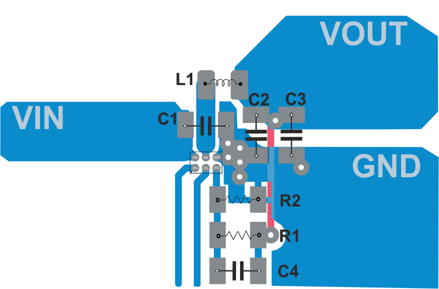
Figure 8-36
PCB Layout of Adjustable Output Voltage Application
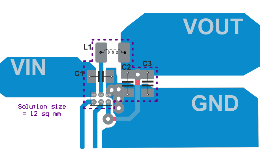
Figure 8-37
PCB Layout of Fixed Output Voltage Application