SLVSDR2B November 2018 – March 2021 ADC12DJ3200QML-SP
PRODUCTION DATA
- 1 Features
- 2 Applications
- 3 Description
- 4 Revision History
- 5 Pin Configuration and Functions
-
6 Specifications
- 6.1 Absolute Maximum Ratings
- 6.2 ESD Ratings
- 6.3 Recommended Operating Conditions
- 6.4 Thermal Information
- 6.5 Electrical Characteristics: DC Specifications
- 6.6 Electrical Characteristics: Power Consumption
- 6.7 Electrical Characteristics: AC Specifications (Dual-Channel Mode)
- 6.8 Electrical Characteristics: AC Specifications (Single-Channel Mode)
- 6.9 Timing Requirements
- 6.10 Switching Characteristics
- 6.11 Timing Diagrams
- 6.12 Typical Characteristics
-
7 Detailed Description
- 7.1 Overview
- 7.2 Functional Block Diagram
- 7.3
Feature Description
- 7.3.1 Analog Inputs
- 7.3.2 ADC Core
- 7.3.3 Timestamp
- 7.3.4 Clocking
- 7.3.5 Digital Down Converters (Dual-Channel Mode Only)
- 7.3.6 JESD204B Interface
- 7.3.7 Alarm Monitoring
- 7.3.8 Temperature Monitoring Diode
- 7.3.9 Analog Reference Voltage
- 7.4
Device Functional Modes
- 7.4.1 Dual-Channel Mode
- 7.4.2 Single-Channel Mode (DES Mode)
- 7.4.3 JESD204B Modes
- 7.4.4 Power-Down Modes
- 7.4.5 Test Modes
- 7.4.6 Calibration Modes and Trimming
- 7.4.7 Offset Calibration
- 7.4.8 Trimming
- 7.4.9 Offset Filtering
- 7.5 Programming
- 7.6 Register Maps
- 8 Application Information Disclaimer
- 9 Layout
- 10Device and Documentation Support
7.3.1 Analog Inputs
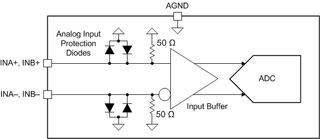
The analog inputs of the ADC12DJ3200QML-SP have internal buffers to enable high input bandwidth and to isolate sampling capacitor glitch noise from the input circuit. Analog inputs must be driven differentially because operation with a single-ended signal results in degraded performance. Both AC-coupling and DC-coupling of the analog inputs is supported. The analog inputs are designed for an input common-mode voltage (VCMI) of 0 V, which is terminated internally through single-ended, 50-Ω resistors to ground (GND) on each input pin. DC-coupled input signals must have a common-mode voltage that meets the device input common-mode requirements specified as VCMI in the Recommended Operating Conditions table. The 0-V input common-mode voltage simplifies the interface to split-supply, fully-differential amplifiers and to a variety of transformers and baluns. The ADC12DJ3200QML-SP includes internal analog input protection to protect the ADC inputs during overranged input conditions; see the Analog Input Protection section. Figure 7-2 shows a simplified analog input model.
 Figure 7-2 ADC12DJ3200QML-SP Analog Input Internal Termination and Protection Diagram
There is minimal degradation in analog input bandwidth when using single-channel mode versus dual-channel mode. In single-channel mode, INA± is strongly recommended to be used as the input to the ADC because ADC performance is optimized for INA±. However, either analog input (INA+ and INA– or INB+ and INB–) can be used. Using INB± results in degraded performance unless custom trim routines are used to optimize performance for INB± in each device. The desired input can be chosen using SINGLE_INPUT in the input mux control register.
INA± is strongly recommended to be used as the input to the ADC in single-channel mode for optimized performance.