SLVSE49B July   2017  – August 2024 ESD401

PRODUCTION DATA  

  1.   1
  2. Features
  3. Applications
  4. Description
  5. Pin Configuration and Functions
  6. Specifications
    1. 5.1 Absolute Maximum Ratings
    2. 5.2 ESD Ratings — JEDEC Specification 
    3. 5.3 ESD Ratings—IEC Specification
    4. 5.4 Recommended Operating Conditions
    5. 5.5 Thermal Information
    6. 5.6 Electrical Characteristics
    7. 5.7 Typical Characteristics
  7. Detailed Description
    1. 6.1 Overview
    2. 6.2 Functional Block Diagram
    3. 6.3 Feature Description
      1. 6.3.1 IEC 61000-4-2 ESD Protection
      2. 6.3.2 IEC 61000-4-4 EFT Protection
      3. 6.3.3 IEC 61000-4-5 Surge Protection
      4. 6.3.4 IO Capacitance
      5. 6.3.5 DC Breakdown Voltage
      6. 6.3.6 Low Leakage Current
      7. 6.3.7 Low ESD Clamping Voltage
      8. 6.3.8 Industrial Temperature Range
      9. 6.3.9 Industry Standard Footprint
    4. 6.4 Device Functional Modes
  8. Application and Implementation
    1. 7.1 Application Information
    2. 7.2 Typical Application
      1. 7.2.1 Design Requirements
      2. 7.2.2 Detailed Design Procedure
        1. 7.2.2.1 Signal Range
        2. 7.2.2.2 Operating Frequency
      3. 7.2.3 Application Curves
    3. 7.3 Power Supply Recommendations
    4. 7.4 Layout
      1. 7.4.1 Layout Guidelines
      2. 7.4.2 Layout Example
  9. Device and Documentation Support
    1. 8.1 Receiving Notification of Documentation Updates
    2. 8.2 Support Resources
    3. 8.3 Trademarks
    4. 8.4 Electrostatic Discharge Caution
    5. 8.5 Glossary
  10. Revision History
  11. 10Mechanical, Packaging, and Orderable Information
    1. 10.1 Tape and Reel Information
  12. 11Mechanical Data

Description

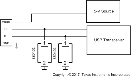
The ESD401 is a bidirectional TVS ESD protection diode featuring low RDYN and low clamping voltage. The ESD401 is rated to dissipate ESD strikes exceeding the maximum level specified in the IEC 61000-4-2 international standard (Level 4). The low dynamic resistance (0.7Ω) to ensure system level protection against transient events. This device features a 0.77pF IO capacitance making it ideal for protecting interfaces such as USB 2.0. The device can operate with ultra-low leakage up to ±5.5V and survive DC faults up to 8.3V.

The ESD401 is offered in the industry standard 0402 (DPY) package.
Package Information
PART NUMBER PACKAGE(1) PACKAGE SIZE(2)
ESD401 DPY (X1SON, 2) 1mm × 0.6mm
For more information, see Section 10.
The package size (length × width) is a nominal value and includes pins, where applicable.
ESD401 Typical
          USB 2.0 Application Schematic Typical USB 2.0 Application Schematic