SLVSE49B
July 2017 – August 2024
ESD401
PRODUCTION DATA
1
1
Features
2
Applications
3
Description
4
Pin Configuration and Functions
5
Specifications
5.1
Absolute Maximum Ratings
5.2
ESD Ratings — JEDEC Specification
5.3
ESD Ratings—IEC Specification
5.4
Recommended Operating Conditions
5.5
Thermal Information
5.6
Electrical Characteristics
5.7
Typical Characteristics
6
Detailed Description
6.1
Overview
6.2
Functional Block Diagram
6.3
Feature Description
6.3.1
IEC 61000-4-2 ESD Protection
6.3.2
IEC 61000-4-4 EFT Protection
6.3.3
IEC 61000-4-5 Surge Protection
6.3.4
IO Capacitance
6.3.5
DC Breakdown Voltage
6.3.6
Low Leakage Current
6.3.7
Low ESD Clamping Voltage
6.3.8
Industrial Temperature Range
6.3.9
Industry Standard Footprint
6.4
Device Functional Modes
7
Application and Implementation
7.1
Application Information
7.2
Typical Application
7.2.1
Design Requirements
7.2.2
Detailed Design Procedure
7.2.2.1
Signal Range
7.2.2.2
Operating Frequency
7.2.3
Application Curves
7.3
Power Supply Recommendations
7.4
Layout
7.4.1
Layout Guidelines
7.4.2
Layout Example
8
Device and Documentation Support
8.1
Receiving Notification of Documentation Updates
8.2
Support Resources
8.3
Trademarks
8.4
Electrostatic Discharge Caution
8.5
Glossary
9
Revision History
10
Mechanical, Packaging, and Orderable Information
10.1
Tape and Reel Information
11
Mechanical Data
7.2
Typical Application
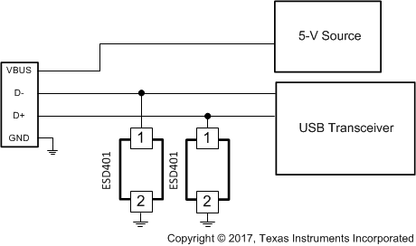
Figure 7-1
USB 2.0 ESD Schematic