SLVSE94G September 2018 – June 2024 TPS2663
PRODUCTION DATA
- 1
- 1 Features
- 2 Applications
- 3 Description
- 4 Device Comparison Table
- 5 Pin Configuration and Functions
- 6 Specifications
- 7 Parameter Measurement Information
-
8 Detailed Description
- 8.1 Overview
- 8.2 Functional Block Diagram
- 8.3
Feature Description
- 8.3.1 Hot Plug-In and Inrush Current Control
- 8.3.2 PGOOD and PGTH
- 8.3.3 Undervoltage Lockout (UVLO)
- 8.3.4 Overvoltage Protection (OVP)
- 8.3.5 Input Reverse Polarity Protection (B_GATE, DRV)
- 8.3.6 Reverse Current Protection
- 8.3.7 Overload and Short-Circuit Protection
- 8.3.8 Output Power Limiting, PLIM (TPS26632, TPS26633, TPS26635, TPS26636, and TPS26637 Only)
- 8.3.9 Current Monitoring Output (IMON)
- 8.3.10 FAULT Response (FLT)
- 8.3.11 IN_SYS, IN, OUT, and GND Pins
- 8.3.12 Thermal Shutdown
- 8.3.13 Low Current Shutdown Control (SHDN)
- 8.4 Device Functional Modes
-
9 Application and Implementation
- 9.1 Application Information
- 9.2
Typical Application: Power Path Protection in a PLC System
- 9.2.1 Design Requirements
- 9.2.2 Detailed Design Procedure
- 9.2.3 Application Curves
- 9.3 System Examples
- 9.4 Dos and Do Nots
- 9.5 Power Supply Recommendations
- 9.6 Layout
- 10Device and Documentation Support
- 11Revision History
- 12Mechanical, Packaging, and Orderable Information
9.3.2 Priority Power MUX Operation
Applications having two energy sources, such as portable battery powered equipment require preference of one source to another. For example, mains power (wall-adapter) has the priority over the internal backup power or auxiliary power. These applications demand for switch over from mains power to backup power only when main input voltage falls below a user defined threshold. The TPS2663x devices provide a simple solution for priority power multiplexing needs.
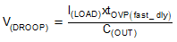
Figure 9-12 shows a typical priority power multiplexing implementation using devices. When the MAIN power is present, the device in VIN_MAIN path powers the OUT bus irrespective of whether auxiliary power VIN_AUX is greater than or less than VIN_MAIN. After the voltage on the VIN_MAIN rail falls below the user-defined threshold, the device VIN_MAIN issues a signal to switch over to auxiliary power VIN_AUX. The transition happens seamlessly in tOVP(dly_fast), with minimal voltage droop on the output. The voltage droop during transition is a function of load current and output capacitance. See Equation 13.
where
- V(DROOP) is in volts, I(LOAD) is load current in Ampere, C(OUT) is output capacitance in µF, tOVP(fast_dly) = 140 µs (typical)
Figure 9-13, Figure 9-14, Figure 9-15 and figure 9-16 show typical switch-over waveforms of Priority Muxing implementation using the TPS26630 or TPS26631 for 20-V primary and 24-V auxiliary bus.
 Figure 9-12 Priority Power Mux Implementation


