SLVSE94G September   2018  – June 2024 TPS2663

PRODUCTION DATA  

  1.   1
  2. Features
  3. Applications
  4. Description
  5. Device Comparison Table
  6. Pin Configuration and Functions
  7. Specifications
    1. 6.1 Absolute Maximum Ratings
    2. 6.2 ESD Ratings
    3. 6.3 Recommended Operating Conditions
    4. 6.4 Thermal Information
    5. 6.5 Electrical Characteristics
    6. 6.6 Timing Requirements
    7. 6.7 Typical Characteristics
  8. Parameter Measurement Information
  9. Detailed Description
    1. 8.1 Overview
    2. 8.2 Functional Block Diagram
    3. 8.3 Feature Description
      1. 8.3.1  Hot Plug-In and Inrush Current Control
        1. 8.3.1.1 Thermal Regulation Loop
      2. 8.3.2  PGOOD and PGTH
        1. 8.3.2.1 PGTH as VOUT Sensing Input
      3. 8.3.3  Undervoltage Lockout (UVLO)
      4. 8.3.4  Overvoltage Protection (OVP)
      5. 8.3.5  Input Reverse Polarity Protection (B_GATE, DRV)
      6. 8.3.6  Reverse Current Protection
      7. 8.3.7  Overload and Short-Circuit Protection
        1. 8.3.7.1 Overload Protection
          1. 8.3.7.1.1 Active Current Limiting at 1 × IOL (TPS26630 and TPS26632 Only)
          2. 8.3.7.1.2 Active Current Limiting With 2 × IOL Pulse Current Support (TPS26631, TPS26633, TPS26635, TPS26636, and TPS26637 Only)
        2. 8.3.7.2 Short-Circuit Protection
          1. 8.3.7.2.1 Start-Up With Short Circuit on Output
      8. 8.3.8  Output Power Limiting, PLIM (TPS26632, TPS26633, TPS26635, TPS26636, and TPS26637 Only)
      9. 8.3.9  Current Monitoring Output (IMON)
      10. 8.3.10 FAULT Response (FLT)
      11. 8.3.11 IN_SYS, IN, OUT, and GND Pins
      12. 8.3.12 Thermal Shutdown
      13. 8.3.13 Low Current Shutdown Control (SHDN)
    4. 8.4 Device Functional Modes
  10. Application and Implementation
    1. 9.1 Application Information
    2. 9.2 Typical Application: Power Path Protection in a PLC System
      1. 9.2.1 Design Requirements
      2. 9.2.2 Detailed Design Procedure
        1. 9.2.2.1 Programming the Current-Limit Threshold—R(ILIM) Selection
        2. 9.2.2.2 Undervoltage Lockout and Overvoltage Set Point
        3. 9.2.2.3 Output Buffer Capacitor – COUT
        4. 9.2.2.4 PGTH Set Point
        5. 9.2.2.5 Setting Output Voltage Ramp Time—(tdVdT)
          1. 9.2.2.5.1 Support Component Selections— RPGOOD and C(IN)
        6. 9.2.2.6 Selecting Q1, Q2 and TVS Clamp for Surge Protection
      3. 9.2.3 Application Curves
    3. 9.3 System Examples
      1. 9.3.1 Simple 24-V Power Supply Path Protection
      2. 9.3.2 Priority Power MUX Operation
      3. 9.3.3 Input Protection for a Compact 24-V Auxiliary Power Supply for Servo Drives
    4. 9.4 Dos and Do Nots
    5. 9.5 Power Supply Recommendations
      1. 9.5.1 Transient Protection
    6. 9.6 Layout
      1. 9.6.1 Layout Guidelines
      2. 9.6.2 Layout Example
  11. 10Device and Documentation Support
    1. 10.1 Documentation Support
      1. 10.1.1 Related Documentation
    2. 10.2 Receiving Notification of Documentation Updates
    3. 10.3 Support Resources
    4. 10.4 Trademarks
    5. 10.5 Electrostatic Discharge Caution
    6. 10.6 Glossary
  12. 11Revision History
  13. 12Mechanical, Packaging, and Orderable Information

Typical Characteristics

–40°C ≤ TA = TJ ≤ +125°C, V(IN_SYS) = V(IN) = 24 V, V( SHDN) = 2 V, R(ILIM) = 30 kΩ, IMON = PGOOD =  FLT = OPEN, C(OUT) = 1 μF, C(dVdT) = OPEN. (Unless stated otherwise)
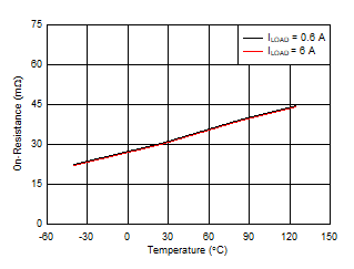
TPS2663 On-Resistance vs Temperature Across Load Current
Figure 6-1 On-Resistance vs Temperature Across Load Current
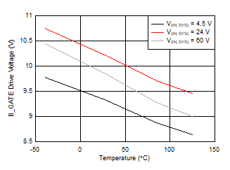
TPS2663 B_GATE Drive Voltage vs Temperature
Figure 6-3 B_GATE Drive Voltage vs Temperature
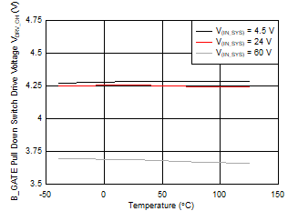
TPS2663 B_GATE Pulldown Drive
                        Voltage vs Temperature
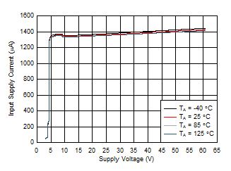
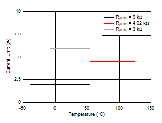
Figure 6-5 B_GATE Pulldown Drive Voltage vs Temperature
TPS2663 Input Supply Current vs Supply Voltage During Normal Operation
Figure 6-7 Input Supply Current vs Supply Voltage During Normal Operation
TPS2663 Overload Current Limit vs Temperature
Figure 6-9 Overload Current Limit vs Temperature
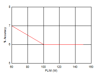
TPS2663 Output Power Limiting Accuracy vs PLIM
Figure 6-11 Output Power Limiting Accuracy vs PLIM
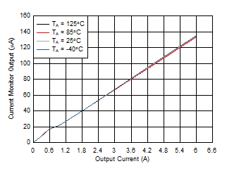
TPS2663 Current Monitor Output vs Output CurrentFigure 6-13 Current Monitor Output vs Output Current
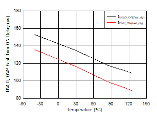
TPS2663 UVLO, OVP Fast Turn-ON
                        Delay vs Temperature
V(PGTH) > V(PGTHF)
Figure 6-15 UVLO, OVP Fast Turn-ON Delay vs Temperature
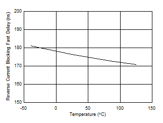
TPS2663 Reverse Current Blocking Response vs Temperature
Figure 6-17 Reverse Current Blocking Response vs Temperature
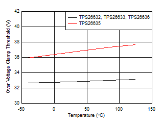
TPS2663 Overvoltage Clamp Threshold vs Temperature
Figure 6-2 Overvoltage Clamp Threshold vs Temperature
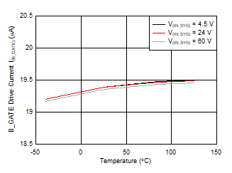
TPS2663 B_GATE Drive Current vs Temperature
Figure 6-4 B_GATE Drive Current vs Temperature
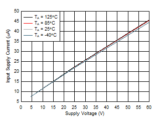
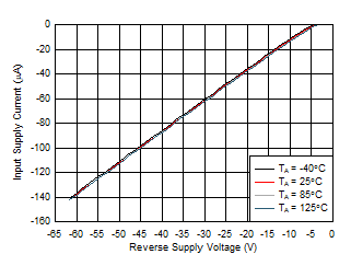
TPS2663 Input Supply Current vs Supply Voltage in Shutdown
Figure 6-6 Input Supply Current vs Supply Voltage in Shutdown
TPS2663 Input Supply Current vs Reverse Supply Voltage,  –V(IN_SYS)
V(OUT) = 0 V
Figure 6-8 Input Supply Current vs Reverse Supply Voltage, –V(IN_SYS)
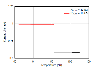
TPS2663 Overload Current Limit vs Temperature
Figure 6-10 Overload Current Limit vs Temperature
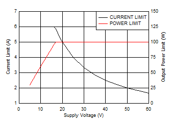
TPS2663 Power Limit, Current limit vs Supply Voltage
TPS26632 R(PLIM) = 100 kΩ R(ILIM) = 3 kΩ
Figure 6-12 Power Limit, Current limit vs Supply Voltage
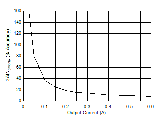
TPS2663 IMON Gain Accuracy at < 0.6-A Output CurrentFigure 6-14 IMON Gain Accuracy at < 0.6-A Output Current
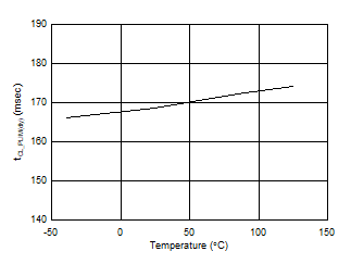
TPS2663 Maximum Duration in Current and Power Limiting vs Temperature
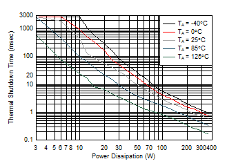
Figure 6-16 Maximum Duration in Current and Power Limiting vs Temperature
TPS2663 Thermal Shutdown Time vs Power Dissipation
Taken on VQFN device on EVM Board
Figure 6-18 Thermal Shutdown Time vs Power Dissipation