SLVSEN9F April   2019  – June 2024 ADC12DJ5200RF

PRODUCTION DATA  

  1.   1
  2. Features
  3. Applications
  4. Description
  5. Pin Configuration and Functions
  6. Specifications
    1. 5.1  Absolute Maximum Ratings
    2. 5.2  ESD Ratings
    3. 5.3  Recommended Operating Conditions
    4. 5.4  Thermal Information
    5. 5.5  Electrical Characteristics: DC Specifications
    6. 5.6  Electrical Characteristics: Power Consumption
    7. 5.7  Electrical Characteristics: AC Specifications (Dual-Channel Mode)
    8. 5.8  Electrical Characteristics: AC Specifications (Single-Channel Mode)
    9. 5.9  Timing Requirements
    10. 5.10 Switching Characteristics
    11. 5.11 Typical Characteristics
  7. Detailed Description
    1. 6.1 Overview
    2. 6.2 Functional Block Diagram
    3. 6.3 Feature Description
      1. 6.3.1  Device Comparison
      2. 6.3.2  Analog Inputs
        1. 6.3.2.1 Analog Input Protection
        2. 6.3.2.2 Full-Scale Voltage (VFS) Adjustment
        3. 6.3.2.3 Analog Input Offset Adjust
      3. 6.3.3  ADC Core
        1. 6.3.3.1 ADC Theory of Operation
        2. 6.3.3.2 ADC Core Calibration
        3. 6.3.3.3 Analog Reference Voltage
        4. 6.3.3.4 ADC Overrange Detection
        5. 6.3.3.5 Code Error Rate (CER)
      4. 6.3.4  Temperature Monitoring Diode
      5. 6.3.5  Timestamp
      6. 6.3.6  Clocking
        1. 6.3.6.1 Noiseless Aperture Delay Adjustment (tAD Adjust)
        2. 6.3.6.2 Aperture Delay Ramp Control (TAD_RAMP)
        3. 6.3.6.3 SYSREF Capture for Multi-Device Synchronization and Deterministic Latency
          1. 6.3.6.3.1 SYSREF Position Detector and Sampling Position Selection (SYSREF Windowing)
          2. 6.3.6.3.2 Automatic SYSREF Calibration
      7. 6.3.7  Programmable FIR Filter (PFIR)
        1. 6.3.7.1 Dual Channel Equalization
        2. 6.3.7.2 Single Channel Equalization
        3. 6.3.7.3 Time Varying Filter
      8. 6.3.8  Digital Down Converters (DDC)
        1. 6.3.8.1 Rounding and Saturation
        2. 6.3.8.2 Numerically-Controlled Oscillator and Complex Mixer
          1. 6.3.8.2.1 NCO Fast Frequency Hopping (FFH)
          2. 6.3.8.2.2 NCO Selection
          3. 6.3.8.2.3 Basic NCO Frequency Setting Mode
          4. 6.3.8.2.4 Rational NCO Frequency Setting Mode
          5. 6.3.8.2.5 NCO Phase Offset Setting
          6. 6.3.8.2.6 NCO Phase Synchronization
        3. 6.3.8.3 Decimation Filters
        4. 6.3.8.4 Output Data Format
        5. 6.3.8.5 Decimation Settings
          1. 6.3.8.5.1 Decimation Factor
          2. 6.3.8.5.2 DDC Gain Boost
      9. 6.3.9  JESD204C Interface
        1. 6.3.9.1 Transport Layer
        2. 6.3.9.2 Scrambler
        3. 6.3.9.3 Link Layer
        4. 6.3.9.4 8B/10B Link Layer
          1. 6.3.9.4.1 Data Encoding (8B/10B)
          2. 6.3.9.4.2 Multiframes and the Local Multiframe Clock (LMFC)
          3. 6.3.9.4.3 Code Group Synchronization (CGS)
          4. 6.3.9.4.4 Initial Lane Alignment Sequence (ILAS)
          5. 6.3.9.4.5 Frame and Multiframe Monitoring
        5. 6.3.9.5 64B/66B Link Layer
          1. 6.3.9.5.1 64B/66B Encoding
          2. 6.3.9.5.2 Multiblocks, Extended Multiblocks and the Local Extended Multiblock Clock (LEMC)
          3. 6.3.9.5.3 Block, Multiblock and Extended Multiblock Alignment using Sync Header
            1. 6.3.9.5.3.1 Cyclic Redundancy Check (CRC) Mode
            2. 6.3.9.5.3.2 Forward Error Correction (FEC) Mode
          4. 6.3.9.5.4 Initial Lane Alignment
          5. 6.3.9.5.5 Block, Multiblock and Extended Multiblock Alignment Monitoring
        6. 6.3.9.6 Physical Layer
          1. 6.3.9.6.1 SerDes Pre-Emphasis
        7. 6.3.9.7 JESD204C Enable
        8. 6.3.9.8 Multi-Device Synchronization and Deterministic Latency
        9. 6.3.9.9 Operation in Subclass 0 Systems
      10. 6.3.10 Alarm Monitoring
        1. 6.3.10.1 Clock Upset Detection
        2. 6.3.10.2 FIFO Upset Detection
    4. 6.4 Device Functional Modes
      1. 6.4.1 Dual-Channel Mode
      2. 6.4.2 Single-Channel Mode (DES Mode)
      3. 6.4.3 Dual-Input Single-Channel Mode (DUAL DES Mode)
      4. 6.4.4 JESD204C Modes
        1. 6.4.4.1 JESD204C Operating Modes Table
        2. 6.4.4.2 JESD204C Modes continued
        3. 6.4.4.3 JESD204C Transport Layer Data Formats
        4. 6.4.4.4 64B/66B Sync Header Stream Configuration
        5. 6.4.4.5 Dual DDC and Redundant Data Mode
      5. 6.4.5 Power-Down Modes
      6. 6.4.6 Test Modes
        1. 6.4.6.1 Serializer Test-Mode Details
        2. 6.4.6.2 PRBS Test Modes
        3. 6.4.6.3 Clock Pattern Mode
        4. 6.4.6.4 Ramp Test Mode
        5. 6.4.6.5 Short and Long Transport Test Mode
          1. 6.4.6.5.1 Short Transport Test Pattern
        6. 6.4.6.6 D21.5 Test Mode
        7. 6.4.6.7 K28.5 Test Mode
        8. 6.4.6.8 Repeated ILA Test Mode
        9. 6.4.6.9 Modified RPAT Test Mode
      7. 6.4.7 Calibration Modes and Trimming
        1. 6.4.7.1 Foreground Calibration Mode
        2. 6.4.7.2 Background Calibration Mode
        3. 6.4.7.3 Low-Power Background Calibration (LPBG) Mode
      8. 6.4.8 Offset Calibration
      9. 6.4.9 Trimming
    5. 6.5 Programming
      1. 6.5.1 Using the Serial Interface
        1. 6.5.1.1 SCS
        2. 6.5.1.2 SCLK
        3. 6.5.1.3 SDI
        4. 6.5.1.4 SDO
        5. 6.5.1.5 Streaming Mode
    6. 6.6 SPI Register Map
  8. Application Information Disclaimer
    1. 7.1 Application Information
    2. 7.2 Typical Applications
      1. 7.2.1 Wideband RF Sampling Receiver
        1. 7.2.1.1 Design Requirements
          1. 7.2.1.1.1 Input Signal Path
          2. 7.2.1.1.2 Clocking
        2. 7.2.1.2 Detailed Design Procedure
          1. 7.2.1.2.1 Calculating Values of AC-Coupling Capacitors
        3. 7.2.1.3 Application Curves
      2. 7.2.2 Reconfigurable Dual-Channel 5-GSPS or Single-Channel 10-Gsps Oscilloscope
        1. 7.2.2.1 Design Requirements
          1. 7.2.2.1.1 Input Signal Path
          2. 7.2.2.1.2 Clocking
          3. 7.2.2.1.3 ADC12DJ5200RF Ososcilloscope Applications
        2. 7.2.2.2 Application Curves
    3. 7.3 Initialization Set Up
    4. 7.4 Power Supply Recommendations
      1. 7.4.1 Power Sequencing
    5. 7.5 Layout
      1. 7.5.1 Layout Guidelines
      2. 7.5.2 Layout Example
  9. Device and Documentation Support
    1. 8.1 Device Support
      1. 8.1.1 Development Support
    2. 8.2 Documentation Support
      1. 8.2.1 Related Documentation
    3. 8.3 Receiving Notification of Documentation Updates
    4. 8.4 Support Resources
    5. 8.5 Trademarks
    6. 8.6 Electrostatic Discharge Caution
    7. 8.7 Glossary
  10. Revision History
  11. 10Mechanical, Packaging, and Orderable Information

Description

The ADC12DJ5200RF device is an RF-sampling, giga-sample, analog-to-digital converter (ADC) that can directly sample input frequencies from DC to above 10GHz. ADC12DJ5200RF can be configured as a dual-channel, 5.2GSPS ADC or single-channel, 10.4GSPS ADC. Support of a useable input frequency range of up to 10GHz enables direct RF sampling of L-band, S-band, C-band, and X-band for frequency agile systems.

The ADC12DJ5200RF uses a high-speed JESD204C output interface with up to 16 serialized lanes supporting up to 17.16Gbps line rate. Deterministic latency and multi-device synchronization is supported through JESD204C subclass-1. The JESD204C interface can be configured to trade-off line rate and number of lanes. Both 8b/10b and 64b/66b data encoding schemes are supported. 64b/66b encoding supports forward error correction (FEC) for improved bit error rates. The interface is backwards compatible with JESD204B receivers.

Innovative synchronization features, including noiseless aperture delay adjustment and SYSREF windowing, simplify system design for multi-channel applications. Optional digital down converters (DDCs) are available to provide digital conversion to baseband and to reduce the interface rate. A programmable FIR filter allows on-chip equalization.
Package Information
PART NUMBER PACKAGE(1) PACKAGE SIZE(2)
ADC12DJ5200RF FCBGA (144) 10mm × 10mm
For more information, Section 10.
The package size (length × width) is a nominal value and includes pins, where applicable.
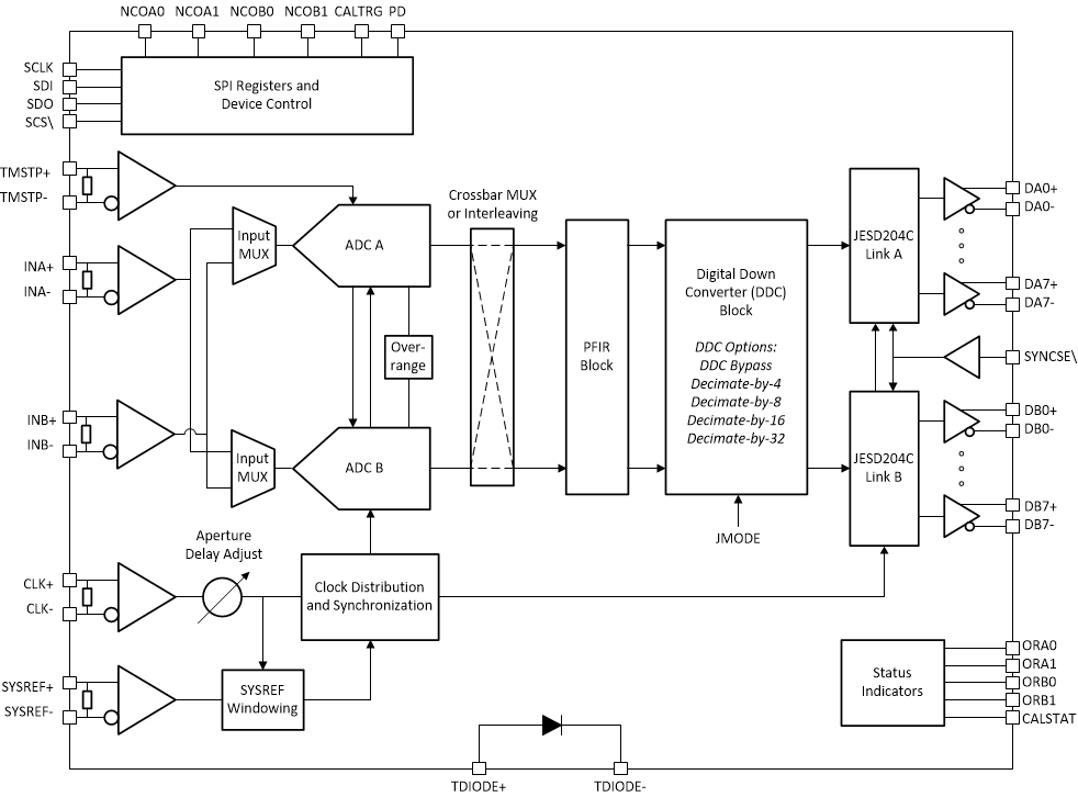
ADC12DJ5200RF ADC12DJ5200RF Block
                    Diagram ADC12DJ5200RF Block Diagram