SLVSEZ5A July 2020 – December 2020 TPS25814
PRODUCTION DATA
- 1 Features
- 2 Applications
- 3 Description
- 4 Revision History
- 5 Pin Configuration and Functions
-
6 Specifications
- 6.1 Absolute Maximum Ratings
- 6.2 ESD Ratings
- 6.3 Recommended Operating Conditions
- 6.4 Recommended Capacitance
- 6.5 Thermal Information
- 6.6 Power Supply Characteristics
- 6.7 Power Consumption
- 6.8 PP_5V Power Switch Characteristics
- 6.9 Power Path Supervisory
- 6.10 CC Cable Detection Parameters
- 6.11 CC VCONN Parameters
- 6.12 Thermal Shutdown Characteristics
- 6.13 Input/Output (I/O) Characteristics
- 6.14 BC1.2 Characteristics
- 6.15 I2C Requirements and Characteristics
- 6.16 Typical Characteristics
- 7 Parameter Measurement Information
-
8 Detailed Description
- 8.1 Overview
- 8.2 Functional Block Diagram
- 8.3 Feature Description
- 8.4 Device Functional Modes
- 9 Application and Implementation
- 10Power Supply Recommendations
- 11Layout
- 12Device and Documentation Support
- 13Mechanical, Packaging, and Orderable Information
8.3.7.1 I2C Interface Description
The TPS25814 supports Standard and Fast mode I2C interfaces. The bidirectional I2C bus consists of the serial clock (SCL) and serial data (SDA) lines. Both lines must be connected to a supply through a pull-up resistor. Data transfer may be initiated only when the bus is not busy.
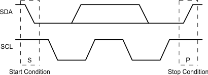
A master sending a Start condition, a high-to-low transition on the SDA input and output, while the SCL input is high initiates I2C communication. After the Start condition, the device address byte is sent, most significant bit (MSB) first, including the data direction bit (R/W).
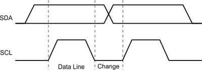
After receiving the valid address byte, this device responds with an acknowledge (ACK), a low on the SDA input/output during the high of the ACK-related clock pulse. On the I2C bus, only one data bit is transferred during each clock pulse. The data on the SDA line must remain stable during the high pulse of the clock period as changes in the data line at this time are interpreted as control commands (Start or Stop). The master sends a Stop condition, a low-to-high transition on the SDA input and output while the SCL input is high.
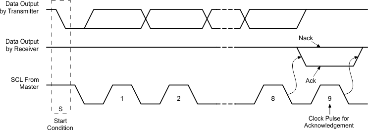
Any number of data bytes can be transferred from the transmitter to receiver between the Start and the Stop conditions. Each byte of eight bits is followed by one ACK bit. The transmitter must release the SDA line before the receiver can send an ACK bit. The device that acknowledges must pull down the SDA line during the ACK clock pulse, so that the SDA line is stable low during the high pulse of the ACK-related clock period. When a slave receiver is addressed, it must generate an ACK after each byte is received. Similarly, the master must generate an ACK after each byte that it receives from the slave transmitter. Setup and hold times must be met to ensure proper operation.
A master receiver signals an end of data to the slave transmitter by not generating an acknowledge (NACK) after the last byte has been clocked out of the slave. The master receiver holding the SDA line high does this. In this event, the transmitter must release the data line to enable the master to generate a Stop condition.
Figure 8-7 shows the start and stop conditions of the transfer. Figure 8-8 shows the SDA and SCL signals for transferring a bit. Figure 8-9 shows a data transfer sequence with the ACK or NACK at the last clock pulse.
 Figure 8-7 I2C Definition of Start and Stop Conditions
 Figure 8-8 I2C Bit Transfer
 Figure 8-9 I2C Acknowledgment