SLVSEZ5A July 2020 – December 2020 TPS25814
PRODUCTION DATA
- 1 Features
- 2 Applications
- 3 Description
- 4 Revision History
- 5 Pin Configuration and Functions
-
6 Specifications
- 6.1 Absolute Maximum Ratings
- 6.2 ESD Ratings
- 6.3 Recommended Operating Conditions
- 6.4 Recommended Capacitance
- 6.5 Thermal Information
- 6.6 Power Supply Characteristics
- 6.7 Power Consumption
- 6.8 PP_5V Power Switch Characteristics
- 6.9 Power Path Supervisory
- 6.10 CC Cable Detection Parameters
- 6.11 CC VCONN Parameters
- 6.12 Thermal Shutdown Characteristics
- 6.13 Input/Output (I/O) Characteristics
- 6.14 BC1.2 Characteristics
- 6.15 I2C Requirements and Characteristics
- 6.16 Typical Characteristics
- 7 Parameter Measurement Information
-
8 Detailed Description
- 8.1 Overview
- 8.2 Functional Block Diagram
- 8.3 Feature Description
- 8.4 Device Functional Modes
- 9 Application and Implementation
- 10Power Supply Recommendations
- 11Layout
- 12Device and Documentation Support
- 13Mechanical, Packaging, and Orderable Information
5 Pin Configuration and Functions
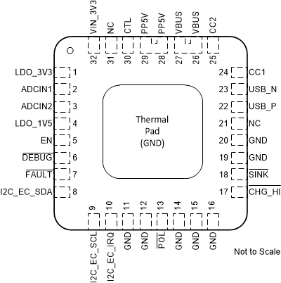
 Figure 5-1 RSM Package32-pin QFNTop View
Table 5-1 Pin Functions
| PIN | TYPE(1) | RESET | Description | |
|---|---|---|---|---|
| NAME | NO. | |||
| ADCIN1 | 2 | I | Hi-Z | Configuration input. Connect to a resistor divider to LDO_3V3. |
| ADCIN2 | 3 | I | Hi-Z | Configuration input. Connect to a resistor divider to LDO_3V3. |
| CC1 | 24 | I/O | Hi-Z | I/O for USB Type-C . |
| CC2 | 25 | I/O | Hi-Z | I/O for USB Type-C . |
| CHG_HI | 17 | I | Hi-Z | Charge logic input to select between minimum or maximum Type-C current advertisement. |
| CTL | 30 | I | Hi-Z | This pin controls which BC 1.2 mode is used. Pull to GND for CDP mode. Pull high for DCP mode. |
| DEBUG | 6 | O | Hi-Z | Open-drain logic output that is asserted low when a Type-C debug accessory is detected. |
| EN | 5 | I | Low | When this pin is pulled low or left floating, the device will be disabled and remain in the Type-C Error Recovery state. |
| FAULT | 7 | O | Hi-Z | Open-drain logic output that asserts when an over-current fault is detected. |
| GND | 11,12,14,15,16,19,20 | — | — | Ground. Connect to ground plane. |
| I2C_EC_SCL | 9 | I | Hi-Z | I2C slave serial clock input. Tie to pullup voltage through a resistor when used or unused. Connect to Embedded Controller (EC). |
| I2C_EC_SDA | 8 | I/O | Hi-Z | I2C slave serial data. Open-drain output. Tie to pullup voltage through a resistor when used or unused. Connect to Embedded Controller (EC). |
| I2C_EC_IRQ | 10 | O | Hi-Z | I2C slave interrupt. Active low. Connect to external voltage through a pull-up resistor. May also be used as a general purpose digital output. Connect to Embedded Controller (EC). |
| LDO_1V5 | 4 | O | — | Output of the CORE LDO. Bypass with capacitance CLDO_1V5 to GND. This pin cannot source current to external circuits. |
| LDO_3V3 | 1 | O | — | Output of supply switched from VIN_3V3 or VBUS LDO. Bypass with capacitance CLDO_3V3 to GND. |
| POL | 13 | O | Hi-Z | Open-drain logic output that gives the information needed to mux the superspeed lines. It is asserted low when CC2 is connected to the cable CC line. |
| PP5V | 28,29 | I | — | 5-V System Supply to VBUS, supply for CCy pins as VCONN. |
| SINK | 18 | O | Hi-Z | Open-drain logic output that asserts low when a Type-C Sink is identified on the CC lines. |
| USB_N | 23 | I/O | Hi-Z | I/O for BC 1.2 functionality. Connect to the USB D- line. |
| USB_P | 22 | I/O | Hi-Z | I/O for BC 1.2 functionality. Connect to the USB D+ line. |
| VBUS | 26,27 | I/O | 5-V to 20-V input. Bypass with capacitance CVBUS to GND. | |
| VIN_3V3 | 32 | I | — | Supply for core circuitry and I/O. Bypass with capacitance CVIN_3V3 to GND. |
| NC | 21,31 | — | — | This pin has no functionality. Leave floating. |
(1) I = input, O = output, I/O = input and output, GPIO = general
purpose digital input and output