SLVSF07F July 2021 – August 2024 TPS7H5001-SP , TPS7H5002-SP , TPS7H5003-SP , TPS7H5004-SP
PRODUCTION DATA
- 1
- 1 Features
- 2 Applications
- 3 Description
- 4 Device Comparison Table
- 5 Device Options
- 6 Pin Configuration and Functions
-
7 Specifications
- 7.1 Absolute Maximum Ratings
- 7.2 ESD Ratings
- 7.3 Recommended Operating Conditions
- 7.4 Thermal Information
- 7.5 Electrical Characteristics: All Devices
- 7.6 Electrical Characteristics: TPS7H5001-SP
- 7.7 Electrical Characteristics: TPS7H5002-SP
- 7.8 Electrical Characteristics: TPS7H5003-SP
- 7.9 Electrical Characteristics: TPS7H5004-SP
- 7.10 Typical Characteristics
-
8 Detailed Description
- 8.1 Overview
- 8.2 Functional Block Diagram
- 8.3
Feature Description
- 8.3.1 VIN and VLDO
- 8.3.2 Start-Up
- 8.3.3 Enable and Undervoltage Lockout (UVLO)
- 8.3.4 Voltage Reference
- 8.3.5 Error Amplifier
- 8.3.6 Output Voltage Programming
- 8.3.7 Soft Start (SS)
- 8.3.8 Switching Frequency and External Synchronization
- 8.3.9 Primary Switching Outputs (OUTA/OUTB)
- 8.3.10 Synchronous Rectifier Outputs (SRA and SRB)
- 8.3.11 Dead Time and Leading Edge Blank Time Programmability (PS, SP, and LEB)
- 8.3.12 Pulse Skipping
- 8.3.13 Duty Cycle Programmability
- 8.3.14 Current Sense and PWM Generation (CS_ILIM)
- 8.3.15 Hiccup Mode Operation (HICC)
- 8.3.16 External Fault Protection (FAULT)
- 8.3.17 Slope Compensation (RSC)
- 8.3.18 Frequency Compensation
- 8.3.19 Thermal Shutdown
- 8.4 Device Functional Modes
-
9 Application and Implementation
- 9.1 Application Information
- 9.2
Typical Application
- 9.2.1 Design Requirements
- 9.2.2
Detailed Design Procedure
- 9.2.2.1 Switching Frequency
- 9.2.2.2 Output Voltage Programming Resistors
- 9.2.2.3 Dead Time
- 9.2.2.4 Leading Edge Blank Time
- 9.2.2.5 Soft-Start Capacitor
- 9.2.2.6 Transformer
- 9.2.2.7 Main Switching FETs
- 9.2.2.8 Synchronous Rectificier FETs
- 9.2.2.9 RCD Clamp
- 9.2.2.10 Output Inductor
- 9.2.2.11 Output Capacitance and Filter
- 9.2.2.12 Sense Resistor
- 9.2.2.13 Hiccup Capacitor
- 9.2.2.14 Frequency Compensation Components
- 9.2.2.15 Slope Compensation Resistor
- 9.2.3 Application Curves
- 9.3 Power Supply Recommendations
- 9.4 Layout
- 10Device and Documentation Support
- 11Revision History
- 12Mechanical, Packaging, and Orderable Information
8.3.16 External Fault Protection (FAULT)
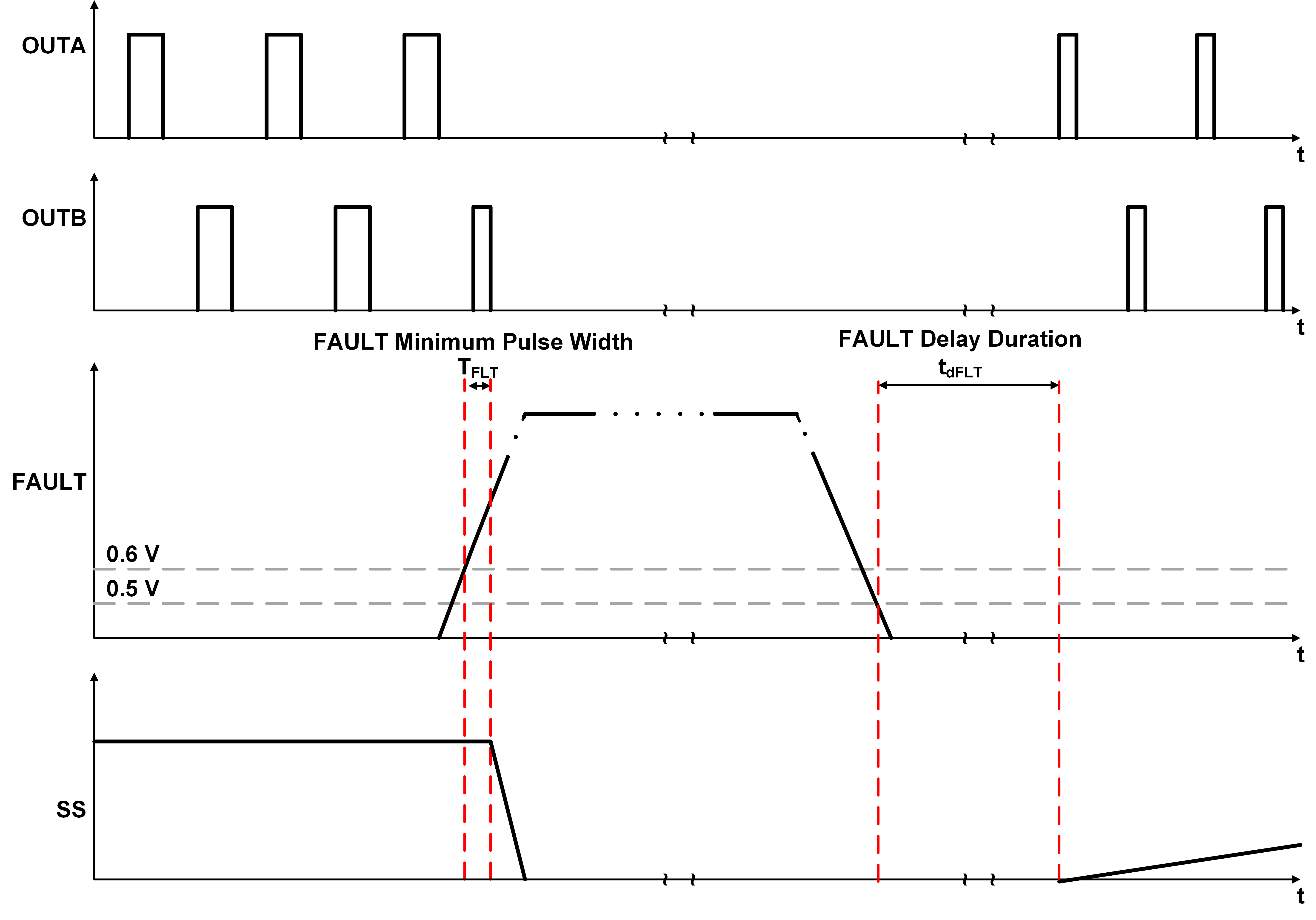
The FAULT pin provides the user with flexibility to implement additional protections for the converter, such as input overcurrent protection or overvoltage protection, if desired. This pin can also be utilized in the event that the user desires more stringent protections than what is offered by the controller (i.e. thermal shutdown). The user can design external logic circuitry to generate the signal necessary to drive this pin based on the protection function. If the voltage on the FAULT pin exceeds 0.6 V (typical) for a duration specified by the FAULT minimum pulse width, a fault shutdown will occur. This FAULT minimum pulse width duration, which is between 0.4 µs and 1.4 µs, is intended to prevent any spurious triggering due to short-term transients. Since any short-term transient event detected on this pin that is less than 1.4 µs in duration may not activate the FAULT pin, these events should be properly evaluated by the user in order to determine the impact to the overall system. Once the fault is detected, the SS pin is discharged and the controller outputs stop switching and stay low as long as the rising threshold is exceeded on the pin. Once the fault has subsided and the voltage of FAULT falls below the falling threshold of 0.5 V (typical), the TPS7H500x-SP enters a delay period that is dependent on the switching frequency. This delay is approximately equal to 15 switching frequency cycles in addition to an internal logic delay. The soft-start sequence is again initiated after the delay period has finished. Equation 15 can be used to determine the length of the fault delay.

In this equation:
- tdFLT is the fault delay duration in μs
- fsw is the switching frequency in kHz
If the FAULT threshold is exceeded during the delay, the entire sequence is started again. Figure 8-16 shows the switching waveforms when the fault mode has been activated in the controller. Note that the OUTB waveforms are only applicable for TPS7H5001-SP and TPS7H5004-SP.
 Figure 8-16 Switching Waveforms During
Fault Mode