SLVSF07F July 2021 – August 2024 TPS7H5001-SP , TPS7H5002-SP , TPS7H5003-SP , TPS7H5004-SP
PRODUCTION DATA
- 1
- 1 Features
- 2 Applications
- 3 Description
- 4 Device Comparison Table
- 5 Device Options
- 6 Pin Configuration and Functions
-
7 Specifications
- 7.1 Absolute Maximum Ratings
- 7.2 ESD Ratings
- 7.3 Recommended Operating Conditions
- 7.4 Thermal Information
- 7.5 Electrical Characteristics: All Devices
- 7.6 Electrical Characteristics: TPS7H5001-SP
- 7.7 Electrical Characteristics: TPS7H5002-SP
- 7.8 Electrical Characteristics: TPS7H5003-SP
- 7.9 Electrical Characteristics: TPS7H5004-SP
- 7.10 Typical Characteristics
-
8 Detailed Description
- 8.1 Overview
- 8.2 Functional Block Diagram
- 8.3
Feature Description
- 8.3.1 VIN and VLDO
- 8.3.2 Start-Up
- 8.3.3 Enable and Undervoltage Lockout (UVLO)
- 8.3.4 Voltage Reference
- 8.3.5 Error Amplifier
- 8.3.6 Output Voltage Programming
- 8.3.7 Soft Start (SS)
- 8.3.8 Switching Frequency and External Synchronization
- 8.3.9 Primary Switching Outputs (OUTA/OUTB)
- 8.3.10 Synchronous Rectifier Outputs (SRA and SRB)
- 8.3.11 Dead Time and Leading Edge Blank Time Programmability (PS, SP, and LEB)
- 8.3.12 Pulse Skipping
- 8.3.13 Duty Cycle Programmability
- 8.3.14 Current Sense and PWM Generation (CS_ILIM)
- 8.3.15 Hiccup Mode Operation (HICC)
- 8.3.16 External Fault Protection (FAULT)
- 8.3.17 Slope Compensation (RSC)
- 8.3.18 Frequency Compensation
- 8.3.19 Thermal Shutdown
- 8.4 Device Functional Modes
-
9 Application and Implementation
- 9.1 Application Information
- 9.2
Typical Application
- 9.2.1 Design Requirements
- 9.2.2
Detailed Design Procedure
- 9.2.2.1 Switching Frequency
- 9.2.2.2 Output Voltage Programming Resistors
- 9.2.2.3 Dead Time
- 9.2.2.4 Leading Edge Blank Time
- 9.2.2.5 Soft-Start Capacitor
- 9.2.2.6 Transformer
- 9.2.2.7 Main Switching FETs
- 9.2.2.8 Synchronous Rectificier FETs
- 9.2.2.9 RCD Clamp
- 9.2.2.10 Output Inductor
- 9.2.2.11 Output Capacitance and Filter
- 9.2.2.12 Sense Resistor
- 9.2.2.13 Hiccup Capacitor
- 9.2.2.14 Frequency Compensation Components
- 9.2.2.15 Slope Compensation Resistor
- 9.2.3 Application Curves
- 9.3 Power Supply Recommendations
- 9.4 Layout
- 10Device and Documentation Support
- 11Revision History
- 12Mechanical, Packaging, and Orderable Information
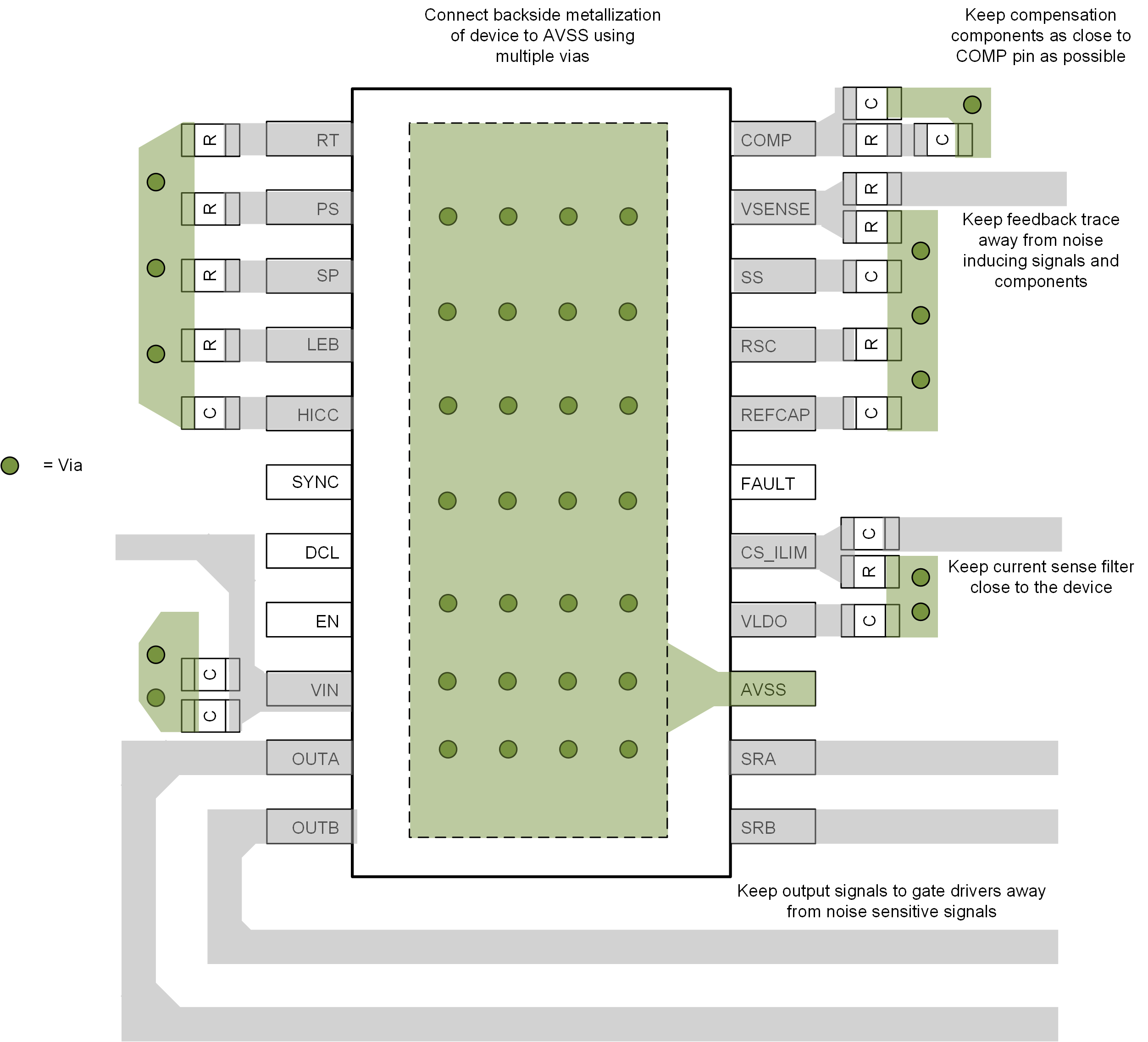
9.4.2 Layout Example
 Figure 9-4 PCB
Layout Example for CFP Package
 Figure 9-5 PCB Layout Example for TSSOP Package