SLVSGZ1A May 2024 – July 2024 DRV8161 , DRV8162
ADVANCE INFORMATION
- 1
- 1 Features
- 2 Applications
- 3 Description
- 4 Device Comparison Table
- 5 Pin Configuration and Functions
- 6 Specification
- 7 Detailed Description
- 8 Application and Implementation
- 9 Layout
- 10Device and Documentation Support
- 11Revision History
- 12Mechanical, Packaging, and Orderable Information
12.1 Tape and Reel Information
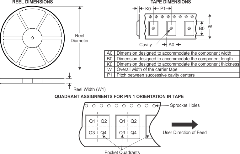
| Device | Package Type | Package Drawing | Pins | SPQ | Reel Diameter (mm) | Reel Width W1 (mm) | A0 (mm) | B0 (mm) | K0 (mm) | P1 (mm) | W (mm) | Pin1 Quadrant |
|---|---|---|---|---|---|---|---|---|---|---|---|---|
| PDRV8161DGSR | VSSOP | DGS | 20 | 3000 | 330.0 | 16.4 | 5.4 | 5.4 | 1.45 | 8.0 | 13.3 | Q1 |
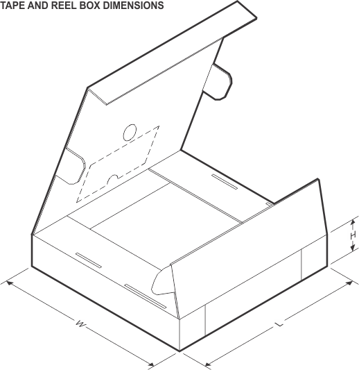
| Device | Package Type | Package Drawing | Pins | SPQ | Length (mm) | Width (mm) | Height (mm) |
|---|---|---|---|---|---|---|---|
| PDRV8161DGSR | VSSOP | DGS | 20 | 3000 | 367.0 | 367.0 | 35.0 |