SLVUBE3B May 2018 – June 2021 TPS56637
5.1 Layout
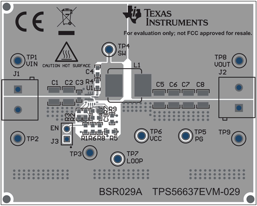
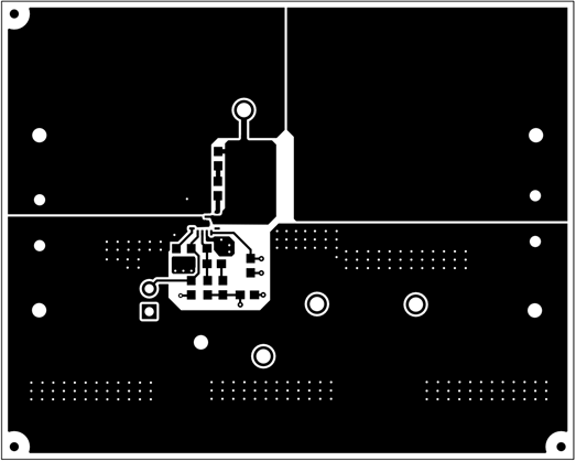
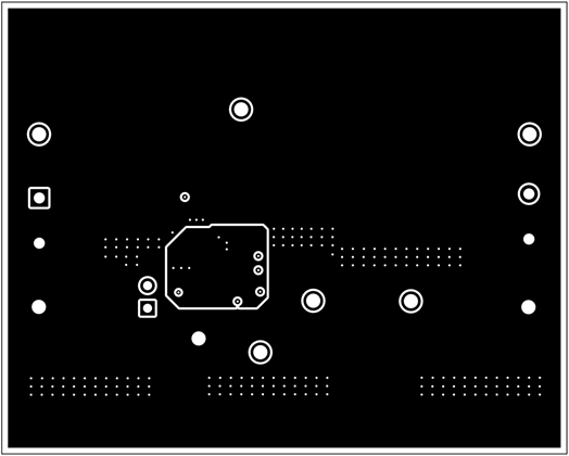
The board layouts for the TPS56637EVM-029 are shown in Figure 5-3, Figure 5-4 and Figure 5-7. The top layer contains the main power traces for VIN, VOUT, and ground. Also on the top layer are connections for the pins of the TPS56637 and a large area filled with ground. Most of the signal traces are also located on the top side. The input decoupling capacitors, C1, C2, and C3 are located as close to the IC as possible. The input and output connectors, test points, and all of the components are located on the top side. GND layer 1, GND layer 2, and the bottom layer are predominantly power ground planes. Analog ground (AGND) area is provided on GND layer 1, GND layer 2, and the bottom layer. Figure 5-7 shows the analog ground (AGND) and power ground (PGND) are connected at a single point on the bottom layer. The bottom layer contains the output voltage feedback trace as well as a connection to the VIN pin of the EN control.
 Figure 5-1 TPS56637EVM-029 Front Photo
 Figure 5-3 Top Assembly
 Figure 5-5 GND Layer 1
 Figure 5-7 Bottom Layer
 Figure 5-2 TPS56637EVM-029 Back Photo
 Figure 5-4 Top Layer
 Figure 5-6 GND Layer 2