SLVUBZ2A September   2020  – December 2020 LM5127-Q1


  1.   Trademarks
  2. 1Introduction
    1. 1.1 Applications
    2. 1.2 Features
  3. 2EVM Setup
    1. 2.1 EVM Characteristics
  4. 3EVM Photo
  5. 4Testing Procedures
    1. 4.1 EVM Connectors and Test Points
  6. 5Test Results
    1. 5.1 Efficiency
    2. 5.2 Thermal Performance
    3. 5.3 Steady State
    4. 5.4 Load Transient
    5. 5.5 Line Transient Responses
  7. 6Schematics, PCB Layers, and Bill of Materials
    1. 6.1 Schematics
    2. 6.2 PCB Layers
    3. 6.3 Bill of Materials
  8. 7EVM Modifications
    1. 7.1 Configure Channel 1 as a Buck Controller
      1. 7.1.1 Component Modifications
      2. 7.1.2 CFG/MODE Pin Selection
    2. 7.2 Configure Channel 2 and Channel 3 as a Dual Phase Buck Controller
      1. 7.2.1 Component Modifications
      2. 7.2.2 CFG/MODE Pin Selection
    3. 7.3 EVM Modification Test Setups
  9. 8Revision History

Line Transient Responses

Section 5.5 presents voltage transients on the input voltage rail (VCH1A). In Figure 5-21 and Figure 5-22, all three channels are enabled, channel 2 is loaded at 5 A and channel 3 is loaded as 7 A.
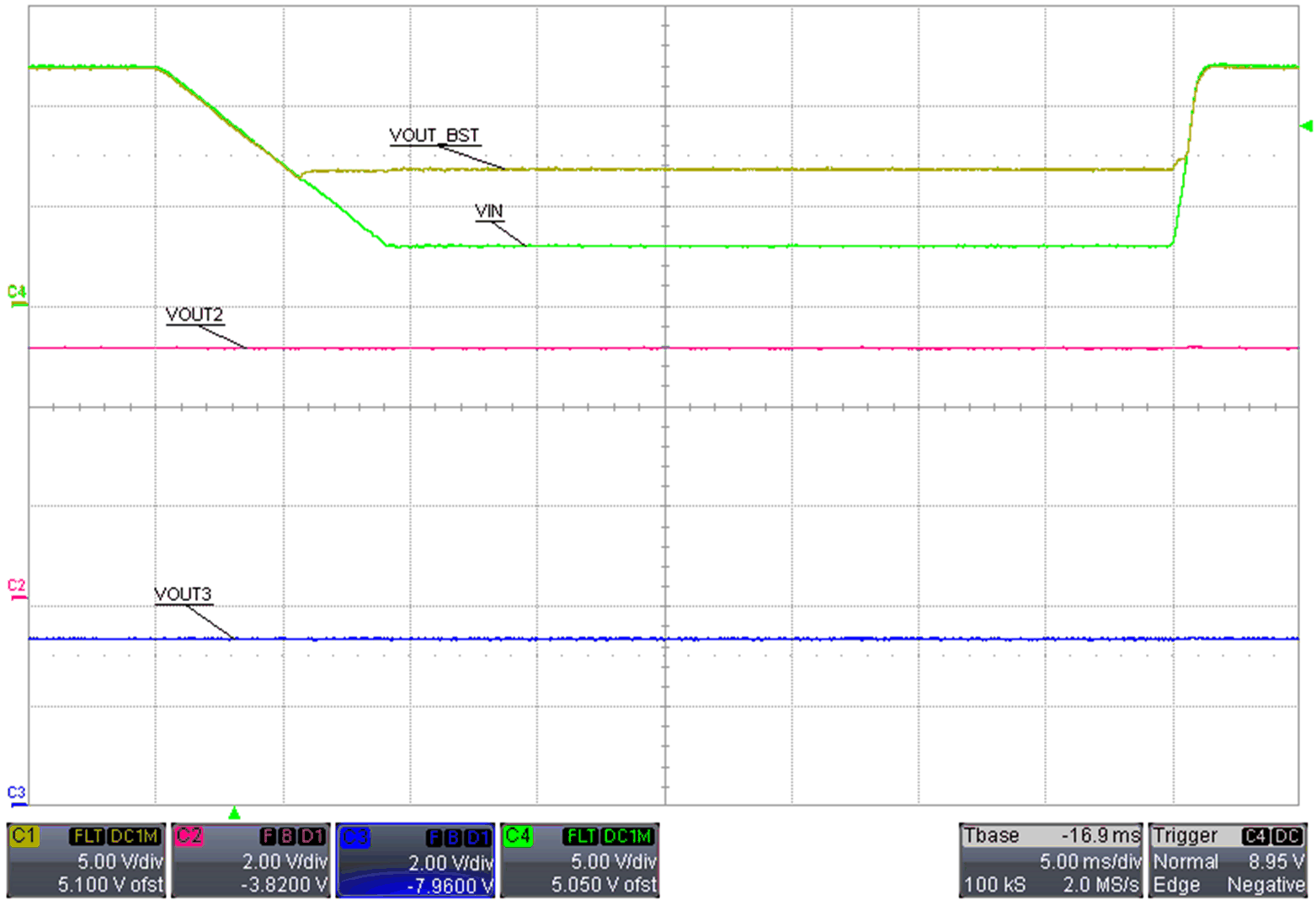
GUID-20200911-CA0I-PTTX-ZFQ0-7HCFMPJDCH67-low.gifFigure 5-21 Cold-Crank Response to VIN = 3 V, IOUT2 = 5 A, IOUT3 = 7 A
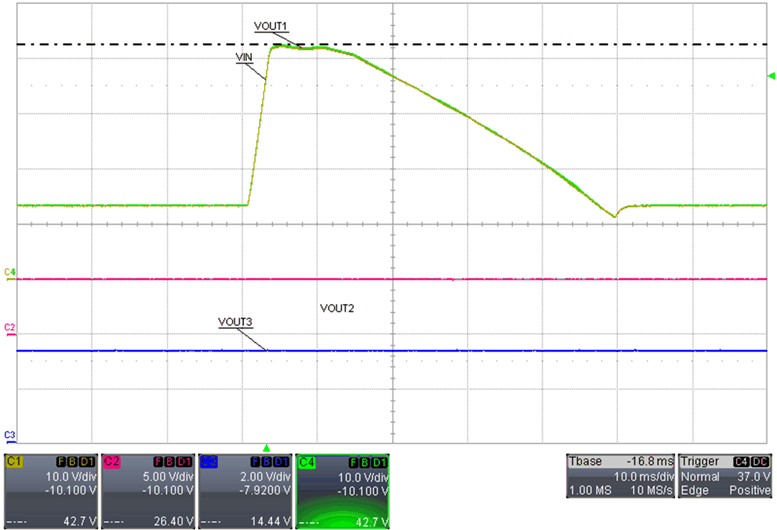
GUID-20200911-CA0I-ZM8J-ZXQ9-MTCMRFMZGWBB-low.gifFigure 5-22 Load Dump Response to VIN = 42 V, IOUT2 = 5 A, IOUT3 = 7 A