SLVUC06 October 2020 TPS650320-Q1
- Trademarks
- 1Introduction
- 2EVM Configurations
- 3Test Points
- 4Graphical User Interface
- 5Typical Performance Plots
- 6TPS650320-Q1 EVM Schematic
- 7TPS650320-Q1 EVM PCB Layers
- 8TPS650320-Q1 EVM Bill of Materials
4.2.4 Device Configuration
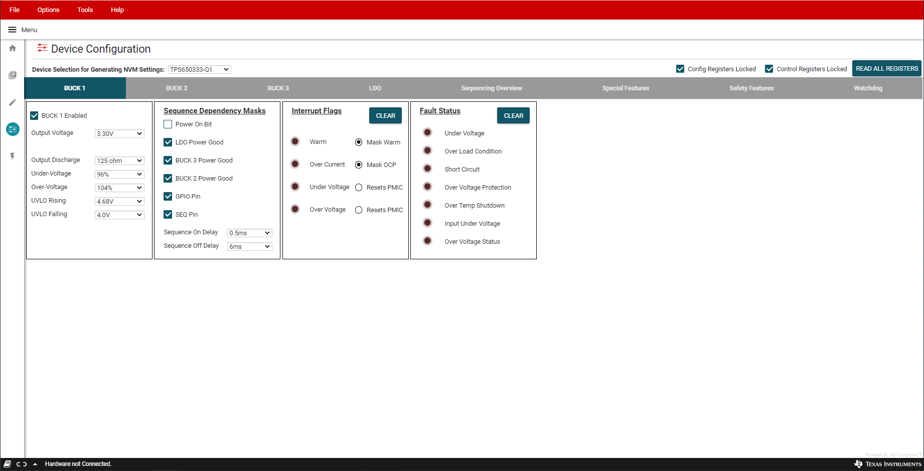
The Device Configuration section is organized into selectable tabs at the top of the page, where only the contents of the blue tab is actively displayed. Each tab contains categorized visual instruments relating to individual bit fields within the register map. Each instrument is linked to the latest bit values in the register map table, and can be used to alter settings within the PMIC through the dropdown menus or check box features. If the Auto Read function in the register map is inactive, the Read All Registers button in the top right area of the Device Configuration page can be used to manually refresh the register page, which will then update the instruments with the latest device values.
The PMIC incorporates Control Lock and Configuration Lock features that can prevent I2C writes to various registers within the device. The status of these locks will always be displayed in the top right hand corner of the Device Configurations page, and can be toggled by clicking their associated checkbox. When the GUI is properly connected to the EVM and write instructions appear to be ignored by the PMIC, confirm the status of these indicators to verify the device is able to accept new write instructions.
 Figure 4-7 TPS6503xx-Q1 GUI Device
Configuration Page