SLVUC06 October   2020 TPS650320-Q1


  1.   Trademarks
  2. 1Introduction
  3. 2EVM Configurations
    1. 2.1 Requirements
    2. 2.2 Operation Instructions
    3. 2.3 Configuring the USB to I2C Adapter
    4. 2.4 Regulator Input Supplies and Features
      1. 2.4.1 Buck 1 Input Supply
      2. 2.4.2 Mid-Vin Buck1 Features
      3. 2.4.3 Buck 2 Input Supply
      4. 2.4.4 Buck 3 Input Supply
      5. 2.4.5 Low-Vin Buck2 and Buck3 Features
      6. 2.4.6 Low Noise LDO Input Supply
      7. 2.4.7 Low Noise LDO Features
    5. 2.5 Selecting the Logic Supply Voltage
  4. 3Test Points
    1. 3.1 Voltage Test Points
  5. 4Graphical User Interface
    1. 4.1 TPS650320-Q1 EVM Debugging
      1. 4.1.1 I2C Communication Port and Adapter Debugging
      2. 4.1.2 Updating MCU Firmware
    2. 4.2 Navigating the GUI
      1. 4.2.1 Home
      2. 4.2.2 Block Diagram
      3. 4.2.3 Registers
      4. 4.2.4 Device Configuration
        1. 4.2.4.1 Using Device Configuration to Define Spin Settings
        2. 4.2.4.2 Configuring the Power Sequence
    3. 4.3 Re-Program PMIC
    4. 4.4 In-Circuit Programming
  6. 5Typical Performance Plots
    1. 5.1 Power Sequence Plots
    2. 5.2 Load Transient Plots
    3. 5.3 Output Voltage Ripple Plots
    4. 5.4 Efficiency Plots
    5. 5.5 LDO Output Noise
  7. 6TPS650320-Q1 EVM Schematic
  8. 7TPS650320-Q1 EVM PCB Layers
  9. 8TPS650320-Q1 EVM Bill of Materials

Block Diagram

The Block Diagram section displays the typical components and functional blocks of the PMIC. A block diagram for the Programming BoosterPack is also shown.
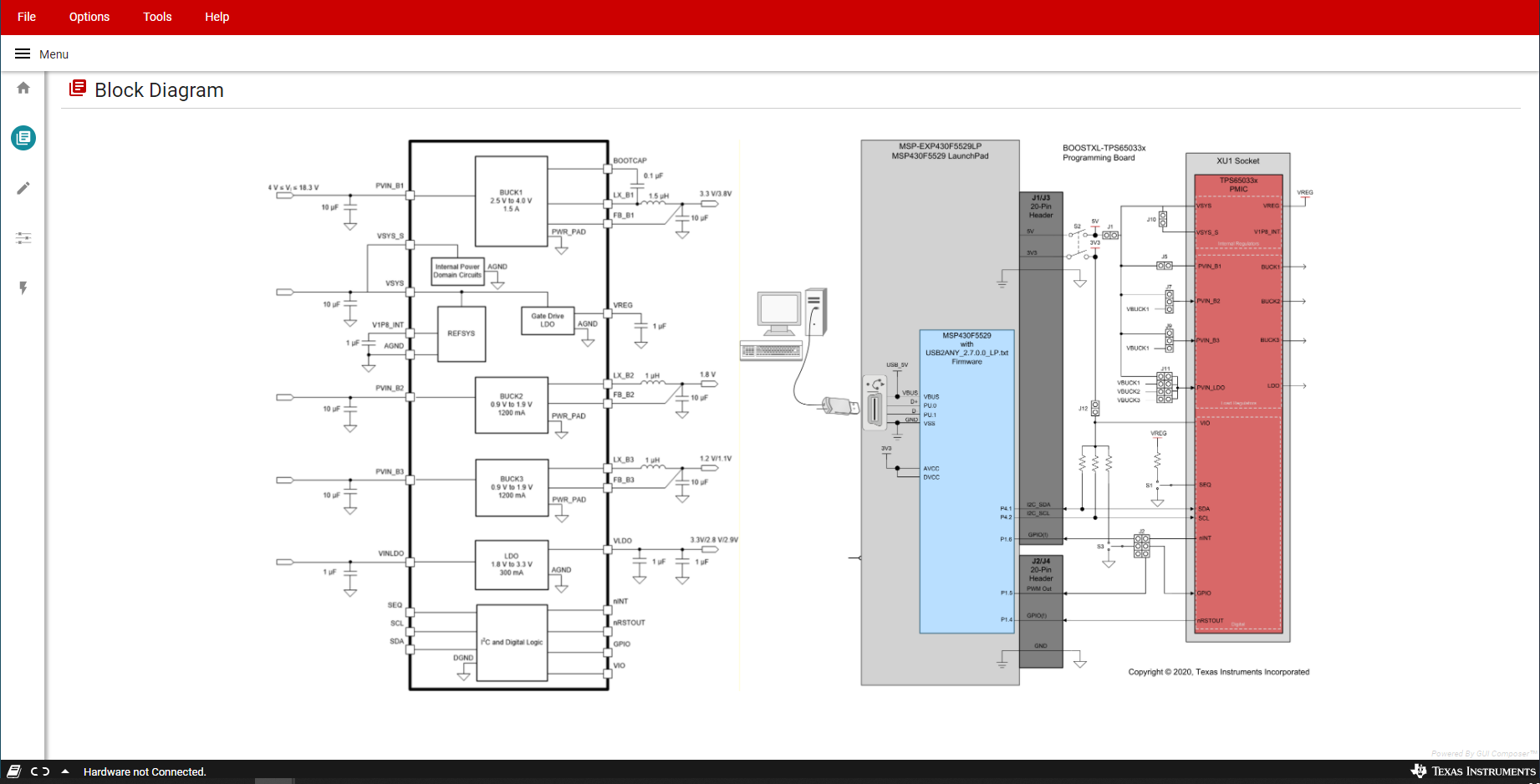
GUID-20200921-CA0I-9W1K-PX30-MFQ8NQ8RFFW5-low.pngFigure 4-5 TPS6503xx-Q1 GUI Block Diagram Page