SLVUC28 August 2022 TPS544C26
5.4 Changing the Output Voltage
SVID Only
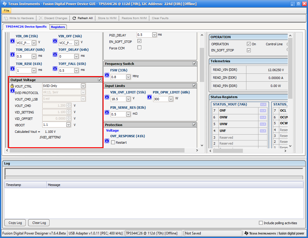
By default, the TPS544C26 VOUT_CTRL is programmed to set the output voltage through SVID Only. With SVID only, the VBOOT setting within the TEMP_MAX (C1h) I2C register sets the initial output voltage after switching is enabled. When configured for SVID only, changing the VBOOT voltage is the only way to change the output voltage in the GUI. If programmed while the device is switching, switching must be disabled then re-enabled for the new VBOOT voltage to take effect.
 Figure 5-5 VOUT_CTRL - SVID Only
SVID VID_SETTING+ I2C VID_OFFSET
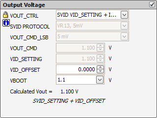
When VOUT_CTRL is programmed for the second setting SVID VID_SETTING+ I2C VID_OFFSET, the VBOOT voltage is the only way to set the output voltage. However, with this setting, the offset can be changed through the GUI with the VID_OFFSET (A8h) I2C register. Switching must be disabled when changing the VID_OFFSET value. If the VID_OFFSET is changed while switching is enabled the TPS544C26 ACKs but the updated value is not be written to the register. When using the 5-mV VID table, the step size of VID_OFFSET is 0.5 mV and when using the 10 mV VID table, the step size of VID_OFFSET is 1 mV.
 Figure 5-6 VOUT_CTRL - SVID and I2C
I2C Only
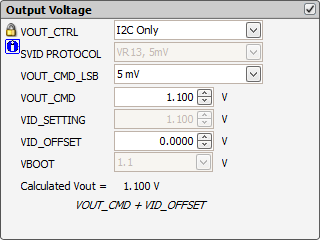
Lastly, when configured for the third setting, I2C Only, the output voltage is programmed through the I2C registers VOUT_CMD (BFh) and VID_OFFSET (A8h). When using this setting, the 5-mV or 10-mV step size of VOUT_CMD is set by the VOUT_CMD_LSB control in the GUI. The VOUT_CMD_LSB control in the GUI adjusts bit 7 in the COMP3 (ADh) I2C register. With this setting, writes to both VOUT_CMD and VID_OFFSET while the device is switching receives an ACK. However, the new value does not take effect until switching is disabled then re-enabled.
 Figure 5-7 VOUT_CTRL - I2C Only