SLVUC49 April   2021 TPS51396A


  1. 1Trademarks
  2. 2Introduction
  3. 3Performance Specification Summary
  4. 4Schematic and List of Materials
  5. 5Board Layout
  6. 6Bench Test Setup conditions
    1. 6.1 Headers Description and Jumper Placement.
    2. 6.2 Power-Up Procedure
  7. 7Test Waveform
    1. 7.1 Power Up
    2. 7.2 Power Down
    3. 7.3 Output Voltage Ripple
    4. 7.4 Load Transient
    5. 7.5 Thermal

Power Down

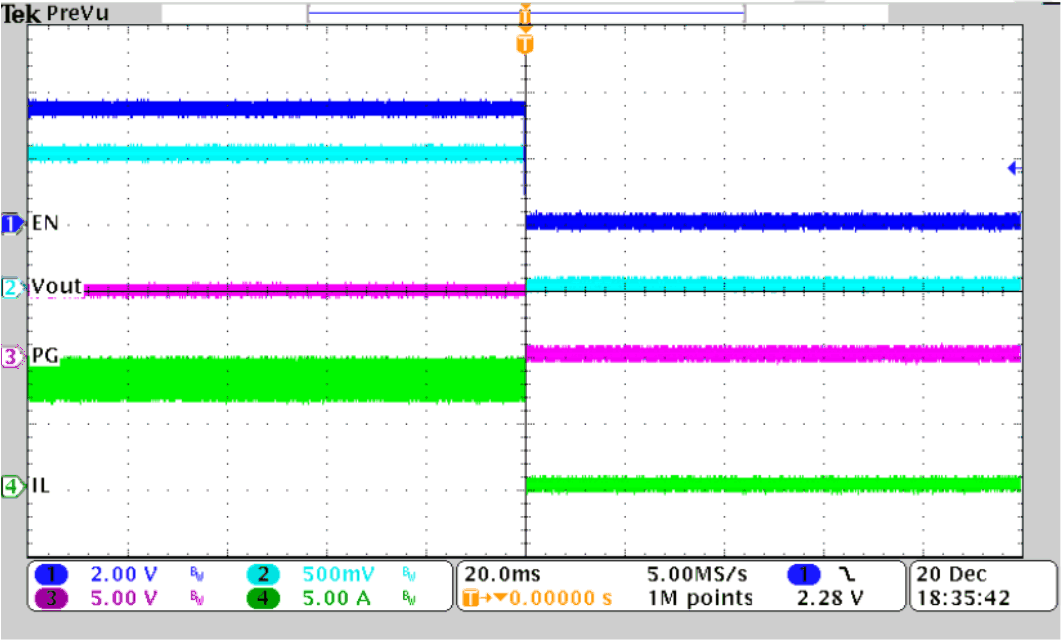
Figure 7-3 and Figure 7-4 show the power down waveforms for the TPS51396AEVM board. The applied input voltage is 12 V. Once the EN is down, Vout ramps down.
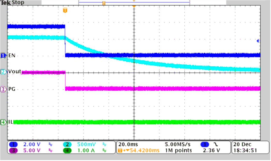
GUID-7F60A2EE-FFDD-490C-86AF-82A275BB9EEF-low.gifFigure 7-3 Power Down with 0 A
GUID-909B32D5-6C1B-4217-9FB1-E9706B8378B5-low.gifFigure 7-4 Power Down with 8 A