SLVUCG3A September 2022 – March 2023 TPSM33625
6 Layout
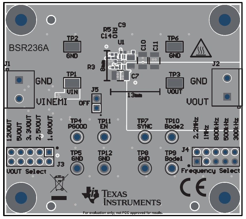
The top silkscreen (that is, J4) differs between the TPSM33625EVM and TPSM3365FEVM, which is the only difference between the layer plots (no routing).
 Figure 6-1 PCB Top 2-D (TPSM33625EVM)
 Figure 6-2 PCB Top 2-D (TPSM33625FEVM)
 Figure 6-3 PCB Bottom 2-D
 Figure 6-4 Top Layer
Reserved for solid ground plane for low-noise and optimized thermal design.
 Figure 6-5 Mid Layer 1
Primary routing layer
 Figure 6-6 Mid Layer 2
Reserved for PI filter and non-critical passive component placement (minus input capacitor). An input capacitor is placed on bottom side of PCB as the input capacitor provides a slightly lower input loop inductance. A single layer implementation is satisfactory as well.
 Figure 6-7 Bottom Layer