SLVUCI4B february 2023 – may 2023 TPS7H5001-SP
3 Test Results
 Figure 3-1 Efficiency vs. Current
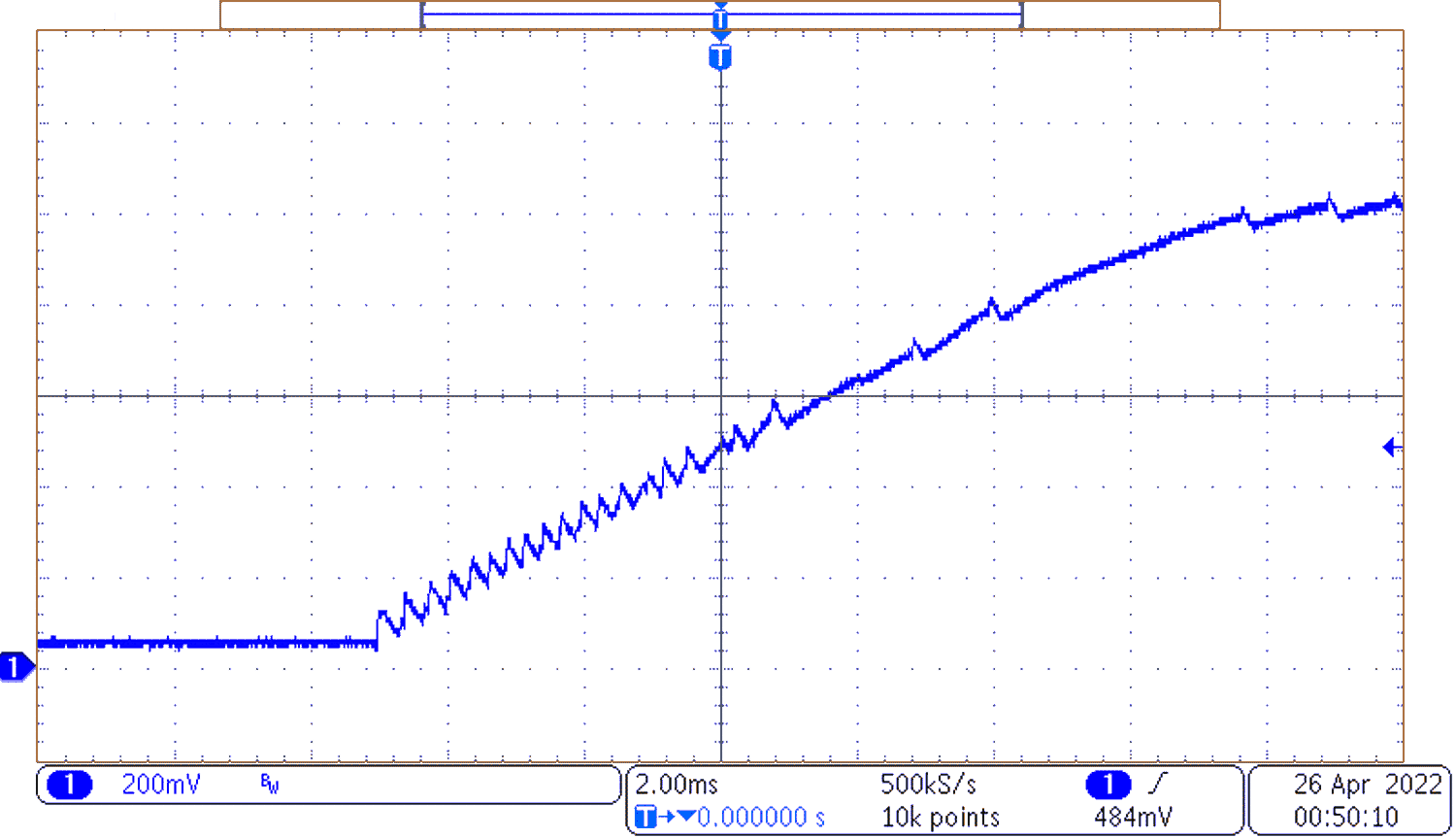 Figure 3-2 Start-up Unloaded
Figure 3-2 shows start-up of the converter when unloaded. The first 4 ms of start-up are choppy due to the minimum on-time of the converter. When the minimum on-time of the converter is smaller than the duty cycle used during parts of start-up choppiness can occur.
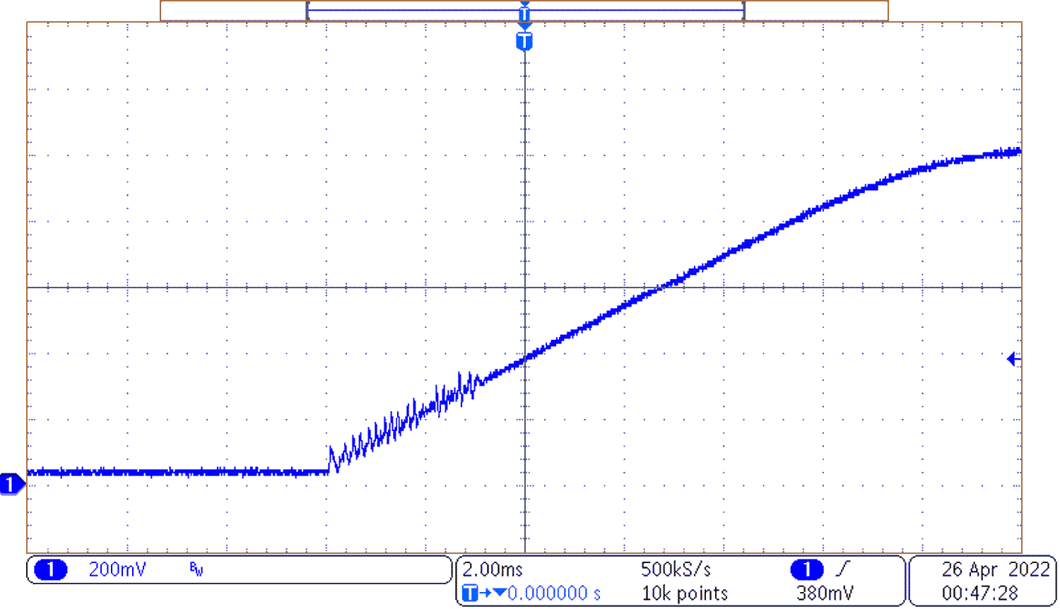 Figure 3-3 Start-up Loaded
Figure 3-3 shows start-up of the converter when loaded with 20 A for the output current. The first 4 ms of start-up are choppy due to the minimum on-time of the converter. When the minimum on-time of the converter is smaller than the duty cycle used during parts of start-up choppiness will occur.
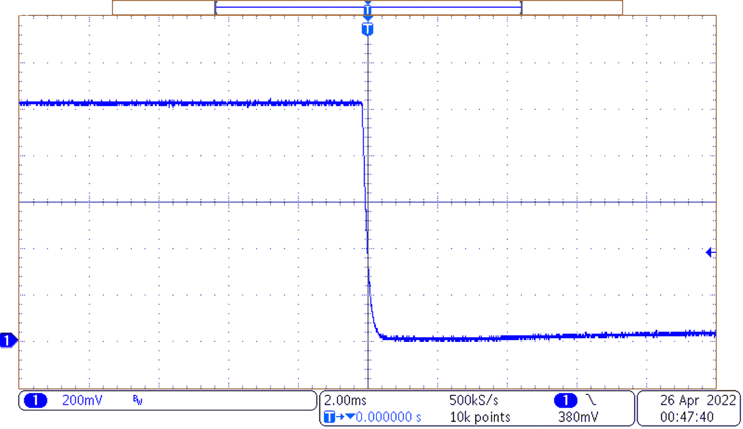 Figure 3-4 Shutdown
Figure 3-4 shows shutdown of the converter when loaded with 20 A on the output current.
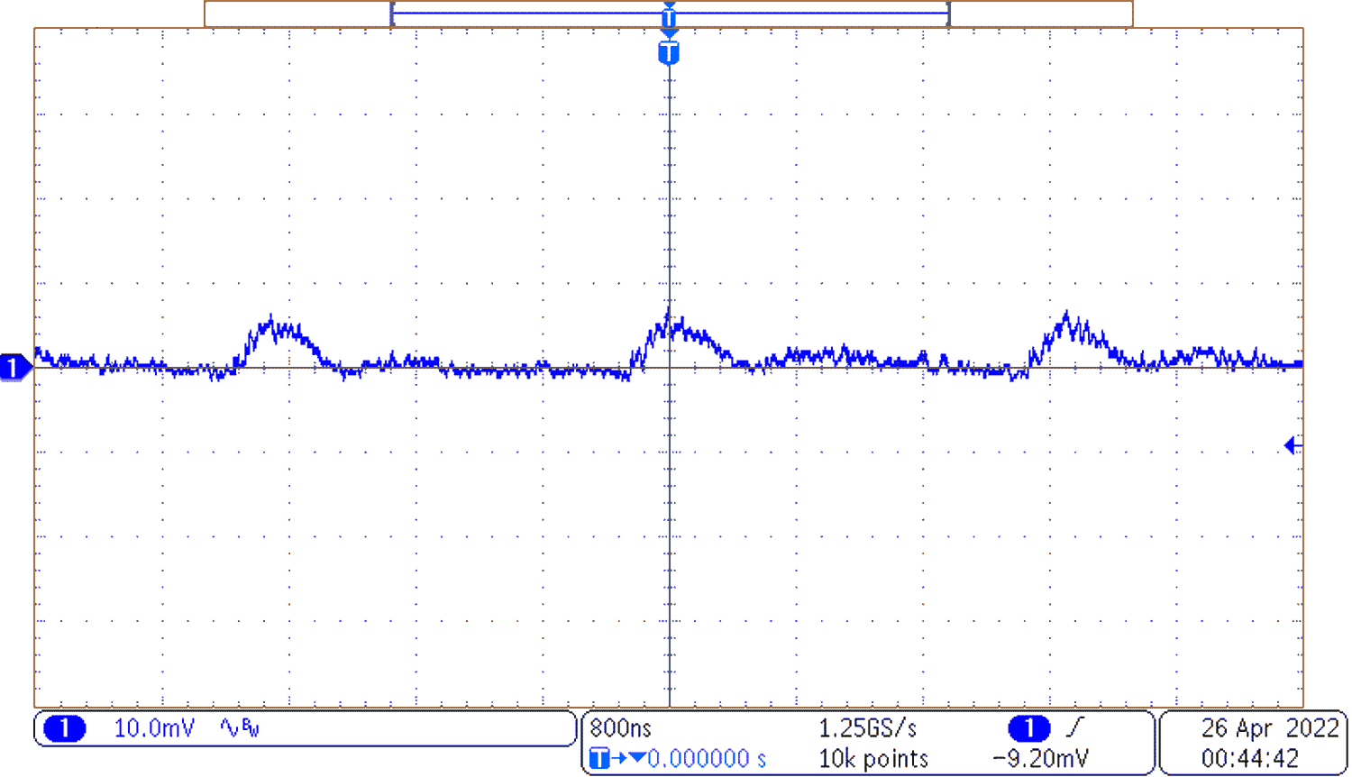 Figure 3-5 Output Voltage Ripple
Figure 3-5 shows the output voltage ripple with an output current of 20 A.
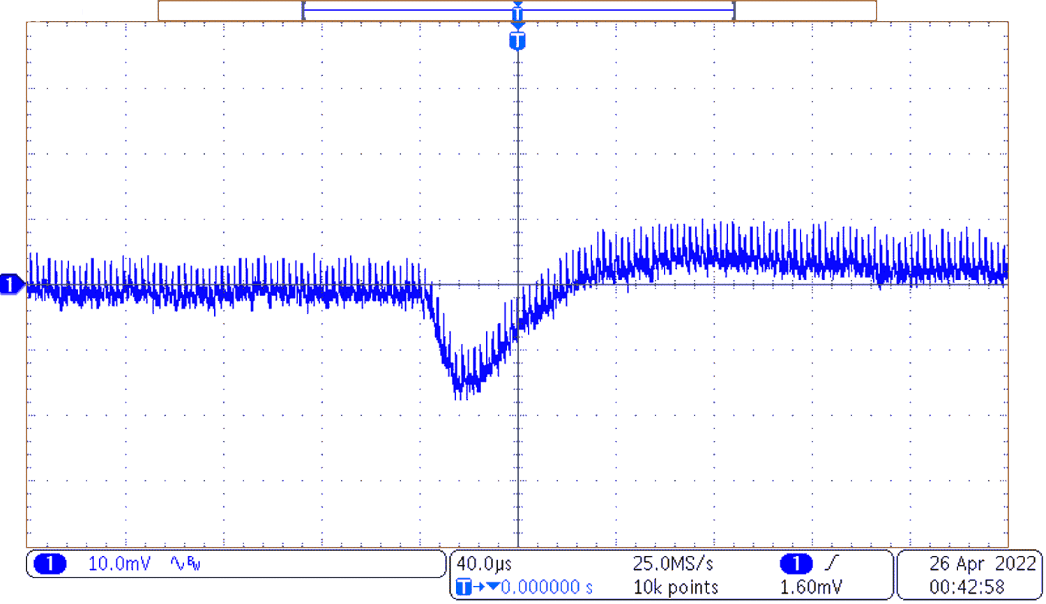 Figure 3-6 Positive Load Step
Figure 3-6 shows the output voltage dip of the converter to a 6.67 positive output current transient.
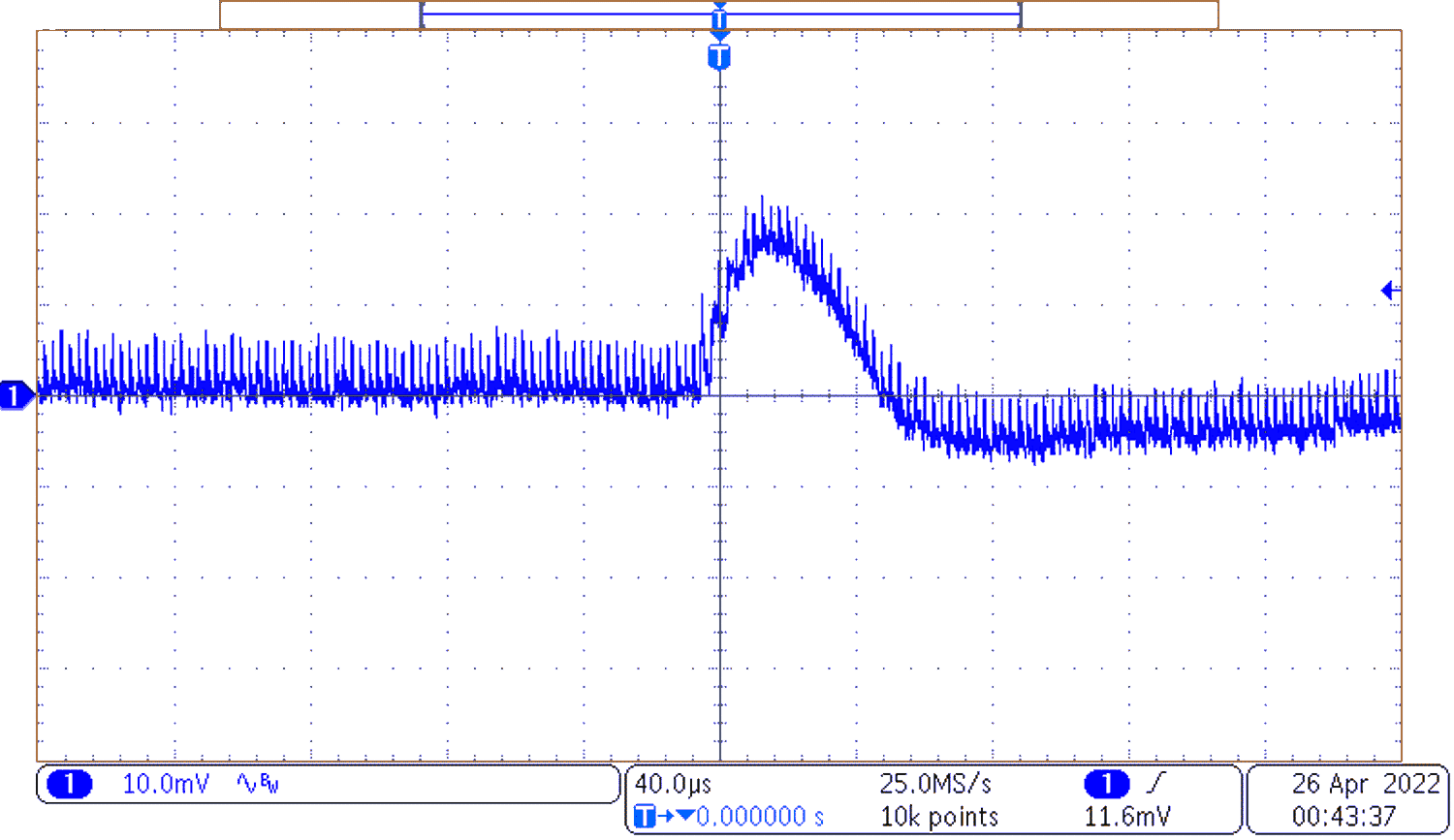 Figure 3-7 Negative Voltage Transient
Figure 3-7 shows the output voltage dip of the converter to a 6.67 positive output current transient.
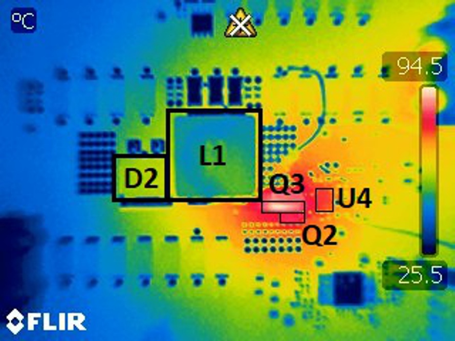 Figure 3-8 Thermal Image of Board with 20 A Output Current
Figure 3-8 shows the thermal image of the board with 20 A output current. The main hot spot of the picture is the bottom side GaN FET. This is the main limiter of the output current. It is suggested to achieve a larger output current that a second GaN FET be put in parallel on the bottom side.
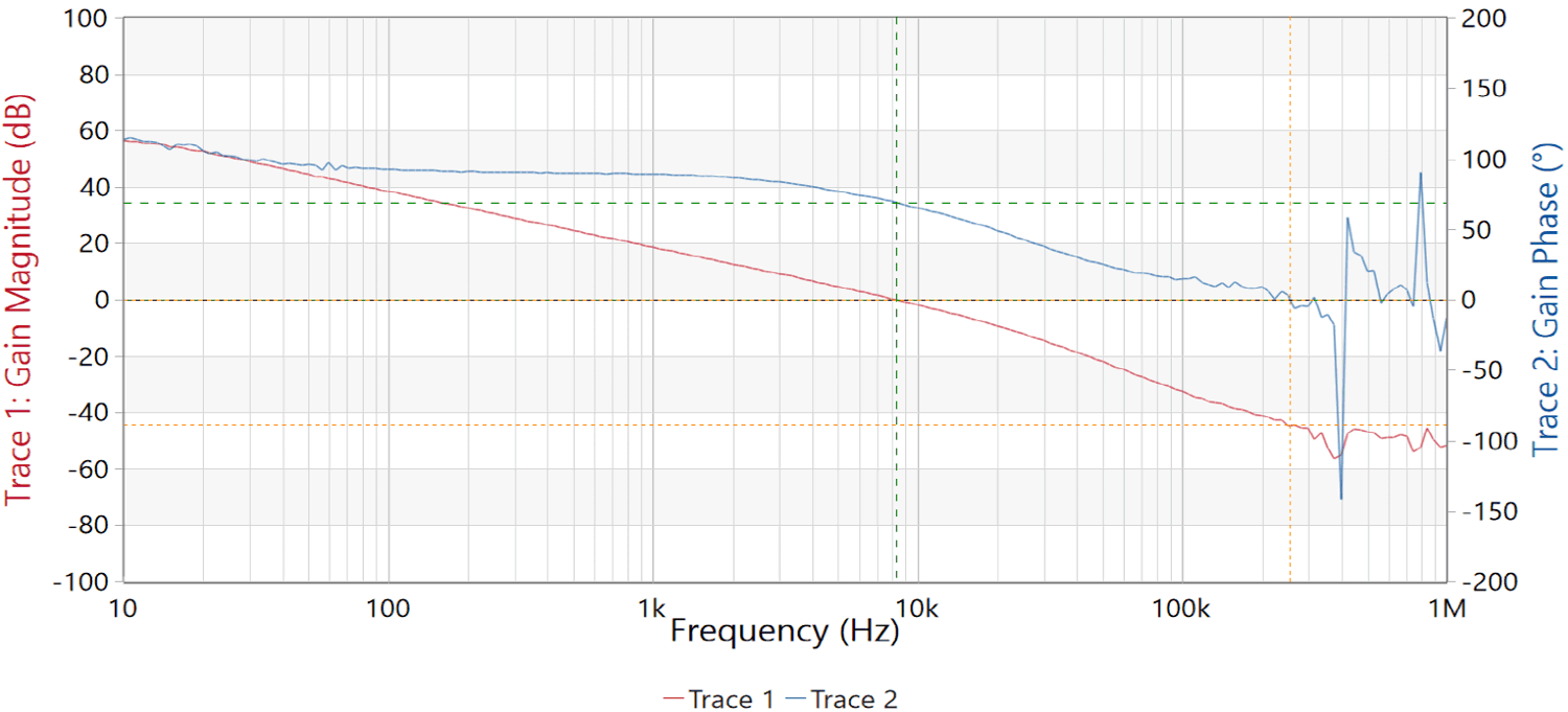 Figure 3-9 Frequency Response
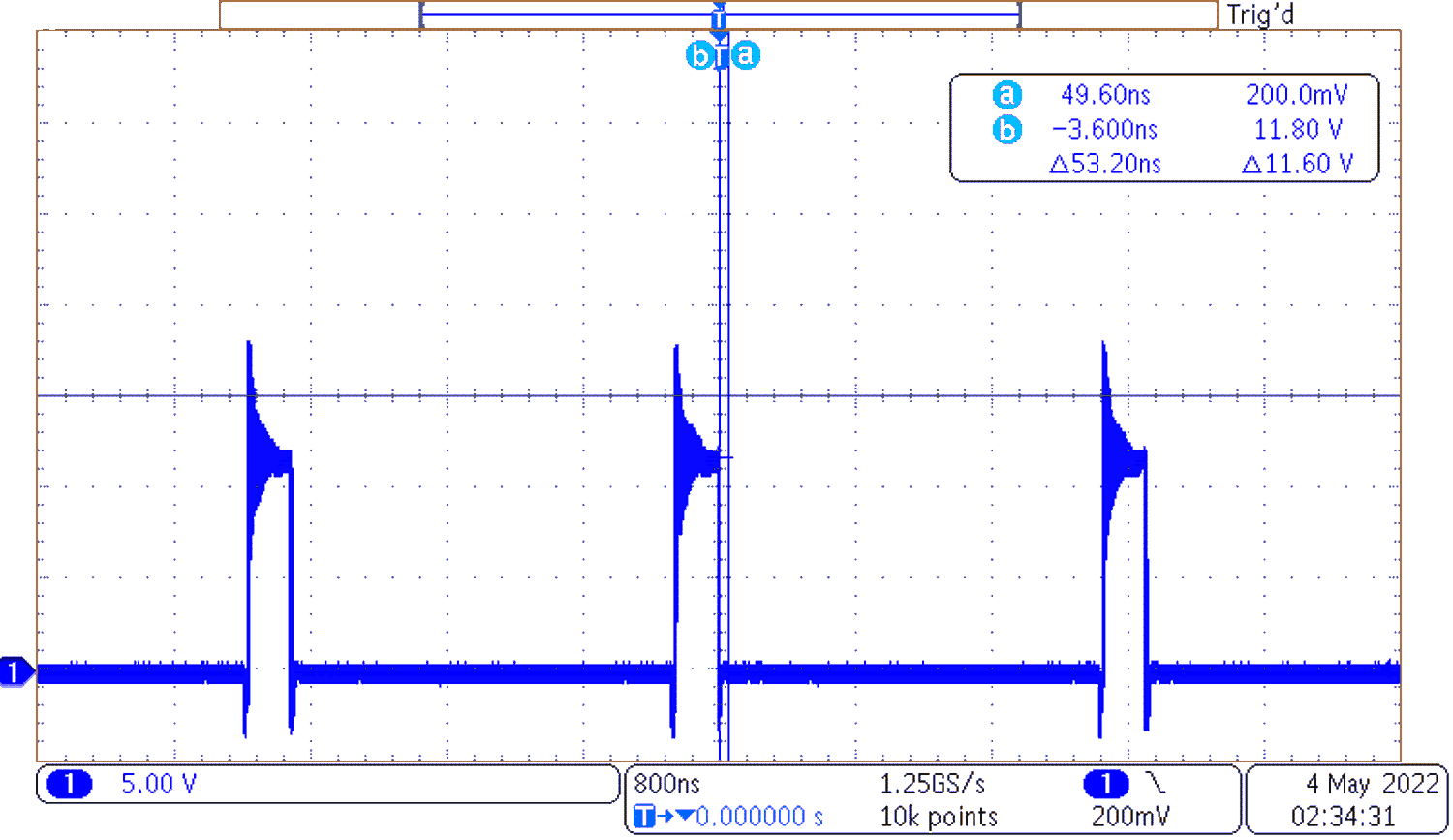 Figure 3-10 Switch Node Voltage with Full
Output Current
Figure 3-10 Switch Node Voltage with Full
Output CurrentFigure 3-10 shows the maximum voltage on the switch node of the converter with an output current of 20 A.