SLVUCN2A October 2023 – August 2024 DRV3901-Q1
2 Hardware Overview
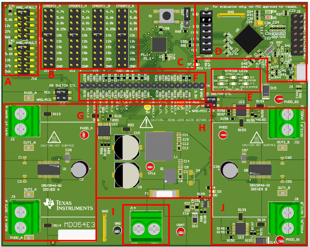
 Figure 2-1 DRV3901-Q1EVM Hardware
Components
Figure 2-1 DRV3901-Q1EVM Hardware
Components| Component | Description |
|---|---|
| A | J3: NAD_nFAULT resistor for Driver A J8: NAD_nFAULT resistor for Driver B |
| B | STATUS LEDs. Refer to Table 2-4 |
| C | J1: S1 button function selection header. Default position set to RST. PUSH function is not supported by firmware but firmware can be modified to perform any desired task when button is pressed and shunt is placed in PUSH position S1: MCU Reset/Push function button. Only MCU Reset function is supported. Press the button to reset MCU when J1 is in RST position. |
| D | J7: Header for serial communication signals (RX, TX) and TDIO or TCK for programming main MCU (U5). Shunts are required for communication between main MCU (U5) and ezFET-LITE debugger. J5: EZFET-LITE flashing connector. Header should be left disconnected. J6: USB connector |
| E | Main signal header. Refer to Table 2-3 |
| F | U1: DRV3901-Q1 Driver A P1: Driver A VREG and PVDD shunt jumper. P3: Driver A VREG and VDRV shunt jumper. |
| G | Reverse battery protection, fuse, and EMI filter circuit |
H | Main power supply (VBAT) connector |
I | U8: DRV3901-Q1 Driver A P2: Driver A VREG and PVDD shunt jumper. P4: Driver A VREG and VDRV shunt jumper. |