SLVUCR7 September 2024 TPS26750
- 1
- Read This First
- 1Introduction
- 2PD Controller Policy Modes
- 3Register Overview
- 4TPS26750 Registers
-
54CC Task Detailed Descriptions
- 5.1 Overview
- 5.2 CPU Control Tasks
- 5.3
PD Message Tasks
- 5.3.1 'SWSk' - PD PR_Swap to Sink
- 5.3.2 'SWSr' - PD PR_Swap to Source
- 5.3.3 'SWDF' - PD DR_Swap to DFP
- 5.3.4 'SWUF' - PD DR_Swap to UFP
- 5.3.5 'GSkC' - PD Get Sink Capabilities
- 5.3.6 'GSrC' - PD Get Source Capabilities
- 5.3.7 'ESkC' - PD EPR Get Sink Capabilities
- 5.3.8 'ESrC' - PD EPR Get Source Capabilities
- 5.3.9 'GPPI' - PD Get Port Partner Information
- 5.3.10 'SSrC' - PD Send Source Capabilities
- 5.3.11 'MBRd' - Message Buffer Read
- 5.4
Patch Bundle Update Tasks
- 5.4.1 'PBMs' - Start Patch Burst Mode Download Sequence
- 5.4.2 'PBMc' - Patch Burst Mode Download Complete
- 5.4.3 'PBMe' - End Patch Burst Mode Download Sequence
- 5.4.4 'GO2P' - Go to Patch Mode
- 5.4.5 'FLrd' - Flash Memory Read
- 5.4.6 'FLad' - Flash Memory Write Start Address
- 5.4.7 'FLwd' - Flash Memory Write
- 5.4.8 'FLvy' - Flash Memory Verify
- 5.5 System Tasks
- 6User Reference
- 7Revision History
6.4 IO_CONFIG Register
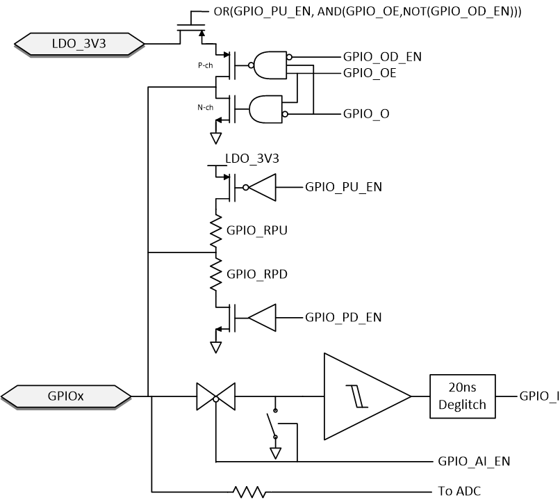
The figure below shows the interface for the GPIO hardware. The register fields GPIO_AI_EN, GPIO_PD_EN, GPIO_PU_EN, GPIO_OE, and GPIO_OD_EN listed in the table below are passed along to the GPIO hardware, independent of the GPIO Event that is configured. The PD controller will then set the signal GPIO_O to high or low to implement the selected output GPIO event. So for example, each output GPIO Event is configurable as push-pull or open-drain using the GPIO_OD_EN bit. For input GPIO events the PD controller will monitor GPIO_I from the figure.
A given GPIO Event can only be assigned to one GPIO pin.
The ProcHot_N_Event GPIO Event can be assigned to any GPIO, but for some PD controllers only a specific GPIO will have the fast reaction time feature (see device data-sheet).
 Figure 6-3 Interface to GPIO hardware.