SLVUCT8 December   2023 TPS6287B10 , TPS6287B15 , TPS6287B20 , TPS6287B25


  1.   1
  2.   Description
  3.   Get Started
  4.   Features
  5.   Applications
  6.   6
  7. 1Evaluation Module Overview
    1. 1.1 Introduction
    2. 1.2 Kit Contents
    3. 1.3 Specification
    4. 1.4 Device Information
  8. 2Hardware
    1. 2.1 Hardware Setup
      1. 2.1.1 Connector Descriptions
      2. 2.1.2 Setup
  9. 3Implementation Results
    1. 3.1 Performance Specification
    2. 3.2 TPS6287B25EVM-024 Test Results
    3. 3.3 Modifications
      1. 3.3.1 Input and Output Capacitors
      2. 3.3.2 Output Voltage Setting
      3. 3.3.3 Control Loop Compensation
      4. 3.3.4 I2C Interface
  10. 4Hardware Design Files
    1. 4.1 Schematic
    2. 4.2 PCB Layout
    3. 4.3 Bill of Materials
  11. 5Additional Information
    1.     Trademarks

PCB Layout

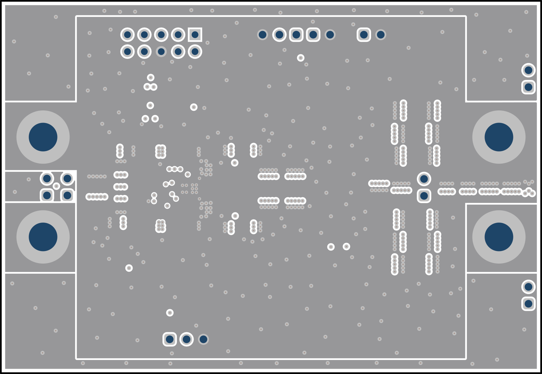
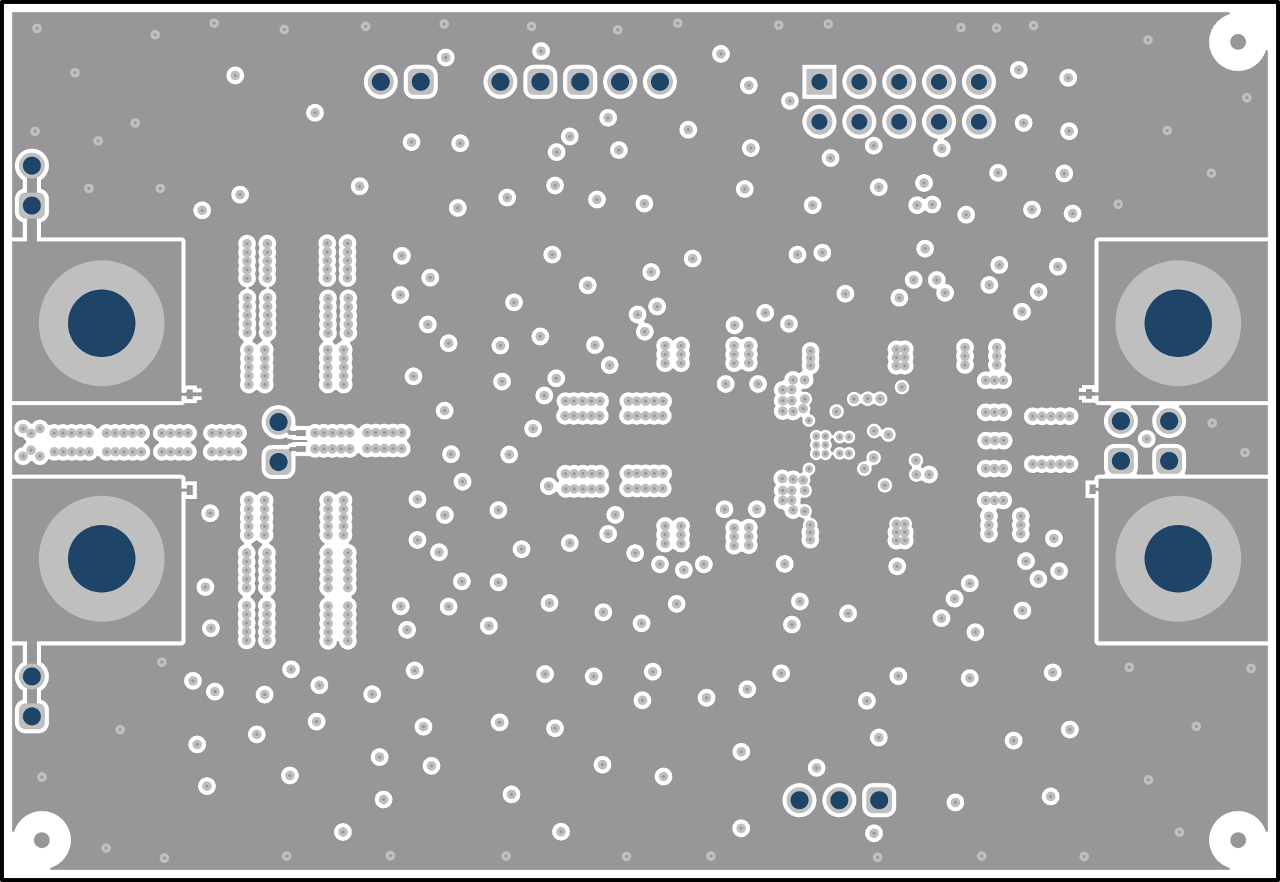
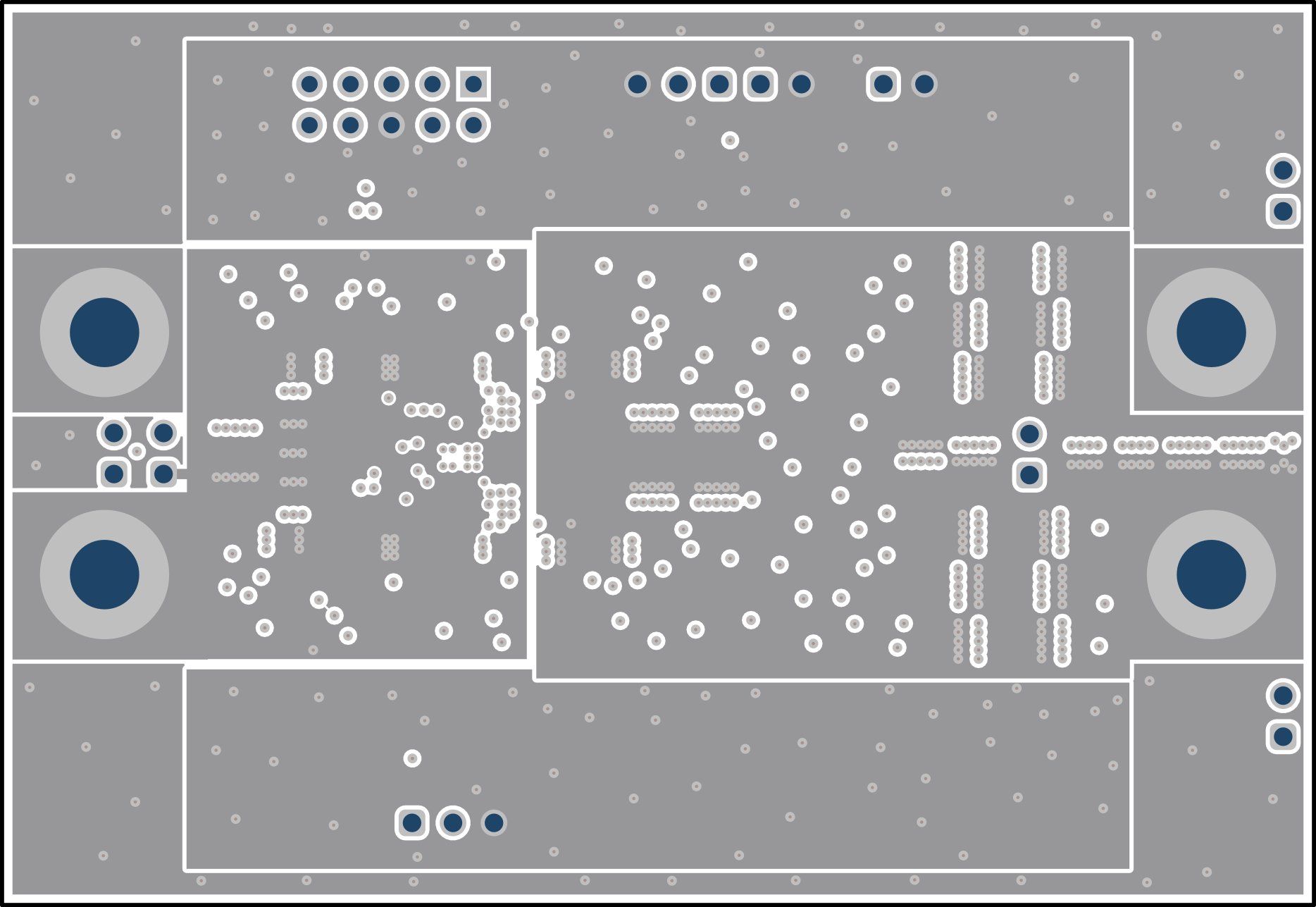
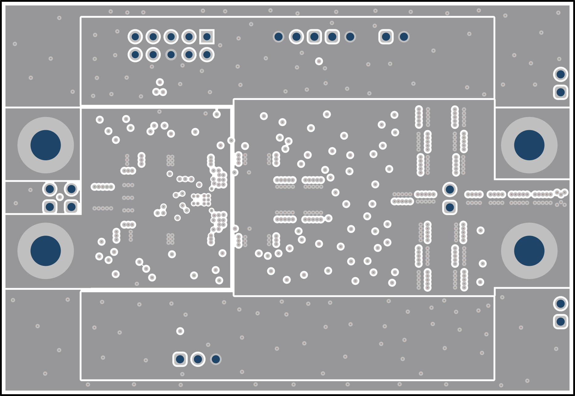
This section provides the TPS6287B25EVM-024 board layout. The gerber files are available on the tool page.
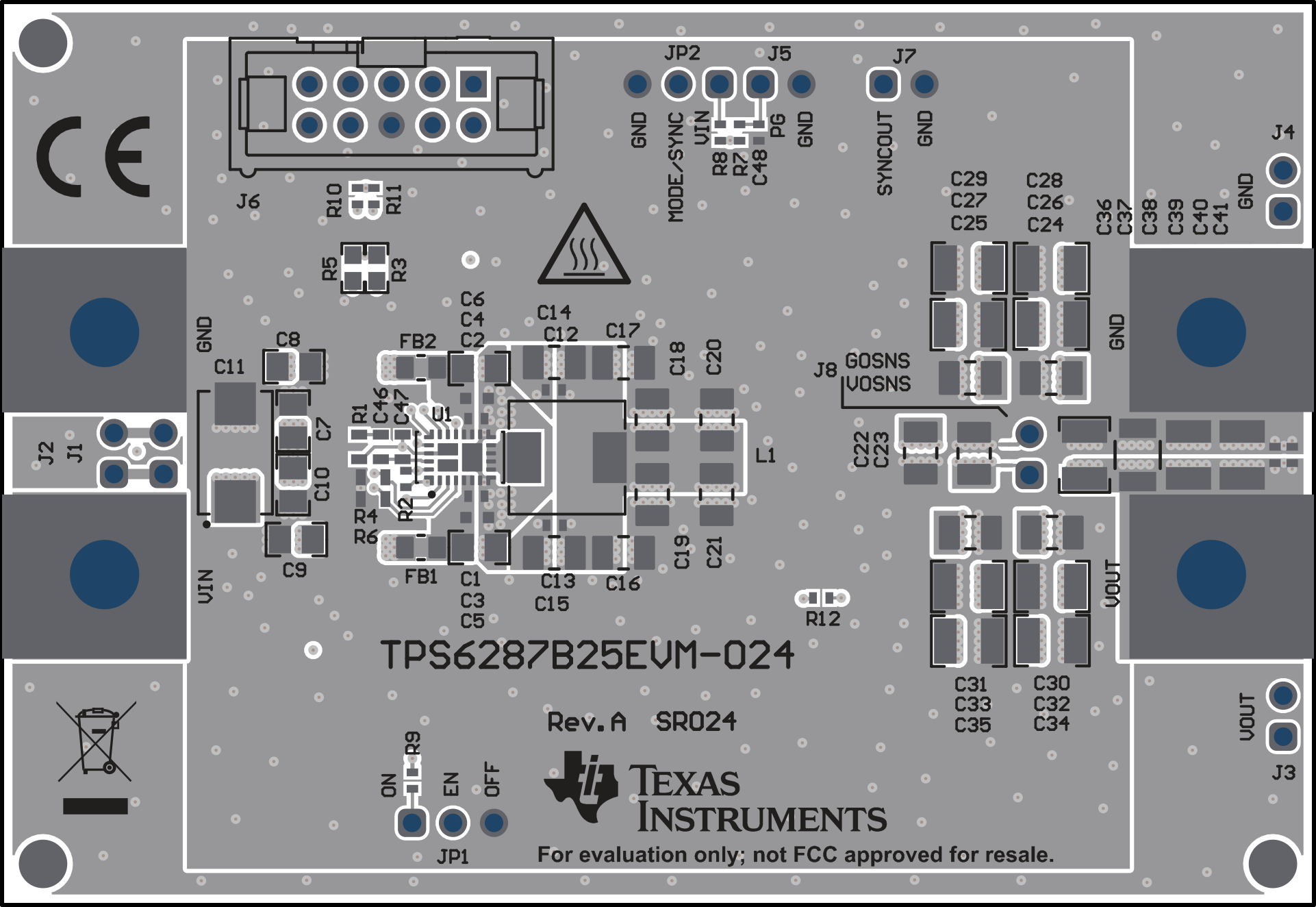
GUID-20231205-SS0I-RLLN-W17H-HQJPHCWG972C-low.pngFigure 4-2 Top Silk
GUID-20231205-SS0I-DHCT-JVNL-KCLDPRWVVCTQ-low.svgFigure 4-4 Layer 2
GUID-20231206-SS0I-WZ3X-M4LC-MBDKPLLS0RTJ-low.svgFigure 4-6 Layer 4
GUID-20231206-SS0I-H06W-XS1Q-SCDQW6KDXDCC-low.pngFigure 4-8 Layer 6
GUID-20231206-SS0I-VPSM-RF54-ZJRCW2B0F3PG-low.pngFigure 4-10 Bottom Layer
GUID-20231206-SS0I-HWKH-20GT-P7RJF0SCNH7C-low.svgFigure 4-3 Top Layer
GUID-20231206-SS0I-25VR-KX0G-LJSFCKVWKRHQ-low.pngFigure 4-5 Layer 3
GUID-20231206-SS0I-7C1J-BWFS-WVNMTP10P7R0-low.pngFigure 4-7 Layer 5
GUID-20231206-SS0I-PRST-NM8H-WC5C7WQTRW8D-low.svgFigure 4-9 Layer 7