SLVUCZ9 July   2024 DRV81004-Q1 , DRV81008-Q1 , DRV81602-Q1 , DRV81620-Q1


  1.   1
  2.   Description
  3.   Get Started
  4.   Features
  5.   Applications
  6.   6
  7. 1Evaluation Module Overview
    1. 1.1 Introduction
    2. 1.2 Kit Contents
    3. 1.3 Specification
    4. 1.4 Device Information
  8. 2Hardware
    1. 2.1 Header Information
    2. 2.2 Connector and Jumper Information
    3. 2.3 Hardware Setup
  9. 3Software
    1. 3.1 Software Setup
    2. 3.2 Web GUI Access or Local GUI Installation
    3. 3.3 Connecting EVM to GUI
    4. 3.4 GUI Overview
      1. 3.4.1 Low-Side Drivers: DRV81004-Q1 and DRV81008-Q1
      2. 3.4.2 High-Side Driver: DRV81080-Q1
      3. 3.4.3 Configurable HS/LS: DRV81602-Q1, DRV81242-Q1, and DRV81620-Q1
  10. 4Hardware Design Files
    1. 4.1 Schematics
    2. 4.2 PCB Layouts
    3. 4.3 Bill of Materials (BOM)
  11. 5Additional Information
    1. 5.1 Known Hardware or Software Issues
    2. 5.2 Trademarks

Low-Side Drivers: DRV81004-Q1 and DRV81008-Q1

The DRV81004-Q1 and DRV81008-Q1 are multi-channel low-side drivers with integrated protection and diagnostic functions. The following images and table can be used as a guide to configure the motor driver through the GUI to control relays and LEDs in automotive and industrial applications.
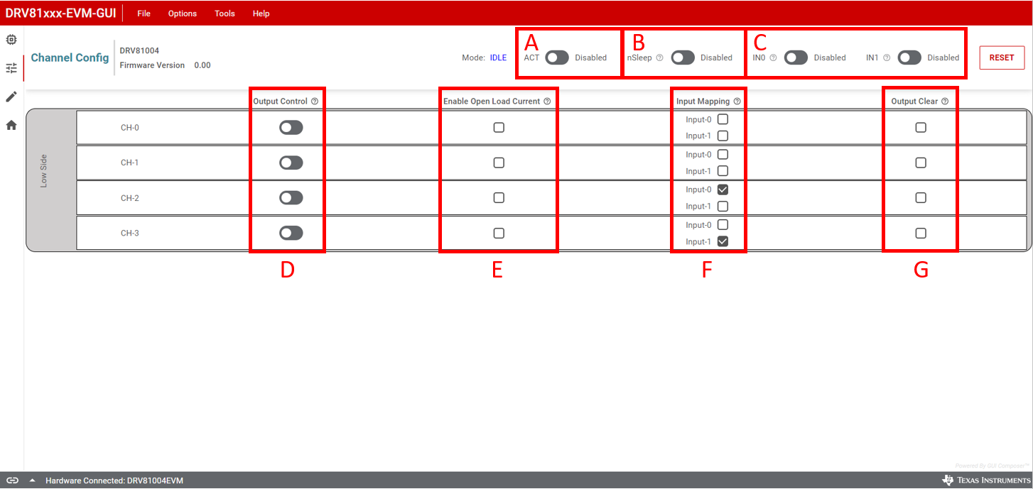
DRV81008-Q1EVM, DRV81602-Q1EVM, DRV81242-Q1EVM,  DRV81004-Q1 GUI Channel
                    Configuration Page Figure 3-6 DRV81004-Q1 GUI Channel Configuration Page
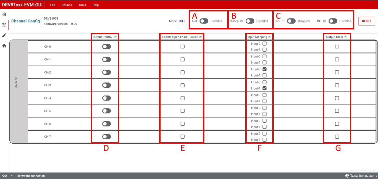
DRV81008-Q1EVM, DRV81602-Q1EVM, DRV81242-Q1EVM,  DRV81008-Q1 GUI Channel
                    Configuration Page Figure 3-7 DRV81008-Q1 GUI Channel Configuration Page
Table 3-1 DRV81004-Q1 and DRV81008-Q1
Component Description

A

Active Mode

  • Disabled (default): device in Idle Mode.
  • Enabled: device in Active Mode.

B

nSLEEP

  • Disabled (default): low-current sleep mode.
  • Enabled: activates Idle mode.

C

Input Pins (IN0 and IN1)

  • Disabled: the input pin is set to logic low.
  • Enabled: the input pin is set to logic high.

D

Output Control

  • Disabled (default): output x is OFF.
  • Enabled: output is ON.

E

Enable Open Load Current

  • Disabled (default): IOL current source not enabled.
  • Enabled: IOL current source enabled.

F

Input Mapping

  • Disabled (default): Output x is not connected to the input pin.
  • Enabled: Output x is connected to the input pin.
Note: By default, IN0 is connected to CH-2 and IN1 is connected to CH-3.

G

Output Clear

  • Disabled (default): normal operation.
  • Enabled: clear the error latch for the selected output.