SLVUD04 August   2024 TPSM83102


  1.   1
  2.   Description
  3.   Features
  4.   4
  5. 1Evaluation Module Overview
    1. 1.1 Introduction
    2. 1.2 Kit Contents
    3. 1.3 Specification
    4. 1.4 Device Information
  6. 2Hardware
    1. 2.1 Background
    2. 2.2 Setup
    3. 2.3 Input and Output Connectors, Test Points, and Headers Description
      1. 2.3.1 J1, Pin 1 and 2 – VIN
      2. 2.3.2 J1, Pin 3 and 4 – S+/S-
      3. 2.3.3 J1, Pin 5 and 6 – GND
      4. 2.3.4 J2, Pin 1 and 2 – VOUT
      5. 2.3.5 J2, Pin 3 and 4 – S+/S-
      6. 2.3.6 J2, Pin 5 and 6 – GND
      7. 2.3.7 Test Points
        1. 2.3.7.1 TP1, TP2
      8. 2.3.8 Header Information
        1. 2.3.8.1 J4– I2C
      9. 2.3.9 Jumper Information
        1. 2.3.9.1 JP1 – ENABLE
    4. 2.4 Setup
    5. 2.5 Modifications
      1. 2.5.1 IC U1 Operation
  7. 3Software
    1. 3.1 Software Setup
    2. 3.2 Interface Hardware Setup
    3. 3.3 User Interface Operation
      1. 3.3.1 Home Screen
      2. 3.3.2 Settings Screen
      3. 3.3.3 Register Map Screen
    4. 3.4 Register Map
      1. 3.4.1 Register CONTROL1 (Target Address: 0x2A; Register Address: 0x02; Default: 0x08)
      2. 3.4.2 Register VOUT (Target Address: 0x2A; Register Address: 0x03; Default: 0x5C)
      3. 3.4.3 Register CONTROL2 (Target Address: 0x2A; Register Address: 0x05; Default:0x45)
  8. 4Hardware Design Files
    1. 4.1 Schematic
    2. 4.2 Board Layout
    3. 4.3 Bill of Materials
  9. 5Additional Information
    1. 5.1 Trademarks

Board Layout

This section provides the TPSM83102EVM-125 board layout and illustrations.

Figure 4-2 and Figure 4-3 show the component placement and PCB layout of the TPSM83102EVM-125.
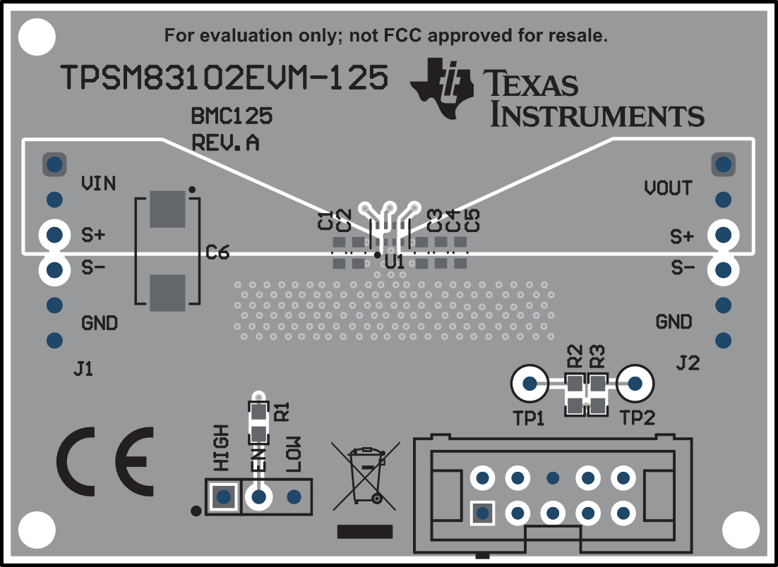
TPSM83102EVM TPSM83102EVM-125 PCB - Top Layer Figure 4-2 TPSM83102EVM-125 PCB - Top Layer
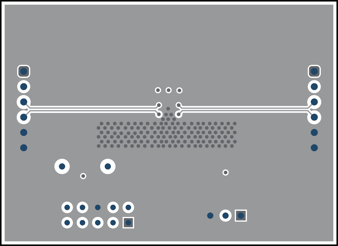
TPSM83102EVM TPSM83102EVM-125 PCB - Bottom Layer (Top View) Figure 4-3 TPSM83102EVM-125 PCB - Bottom Layer (Top View)