SLYT857 August 2024 TPS1200-Q1 , TPS1211-Q1
4 Automatic PWM-based capacitor charging
As shown in Figure 5, the high-side driver outputs in the PCB connect to remote ECUs through lengthy cables varying from 1m to several meters. As an example, a 50A wire (8AWG) harness has 2mΩ-per-meter and 1.5µH-per-meter characteristics. The D1 diode is a part of the system design that allows the freewheel path for the cable harness inductive current. The high-side drivers have strong gate-drive outputs capable of driving FETs in parallel with short (<1µs) turnon and turnoff times, providing overcurrent and short-circuit protection. The cable parasitic, D1 diode and high-side MOSFETs form a typical buck regulator configuration.
During startup, the uncharged output capacitor draws inrush current and triggers a short-circuit event when the inrush current hits the short-circuit protection threshold (ISCP). The high-side driver turns off the power path and reinitiates turnon after a retry period (TAUTO-RETRY). This process continues until the output capacitance is fully charged, as shown in Figure 6, after which the high-side driver goes into normal operation and drives the load.
 Figure 5 Circuit representation for
pulse-width modulation (PWM) charging using a high-side driver.
 Figure 6 PWM charging method conceptual
waveforms during startup.
Figure 6 PWM charging method conceptual
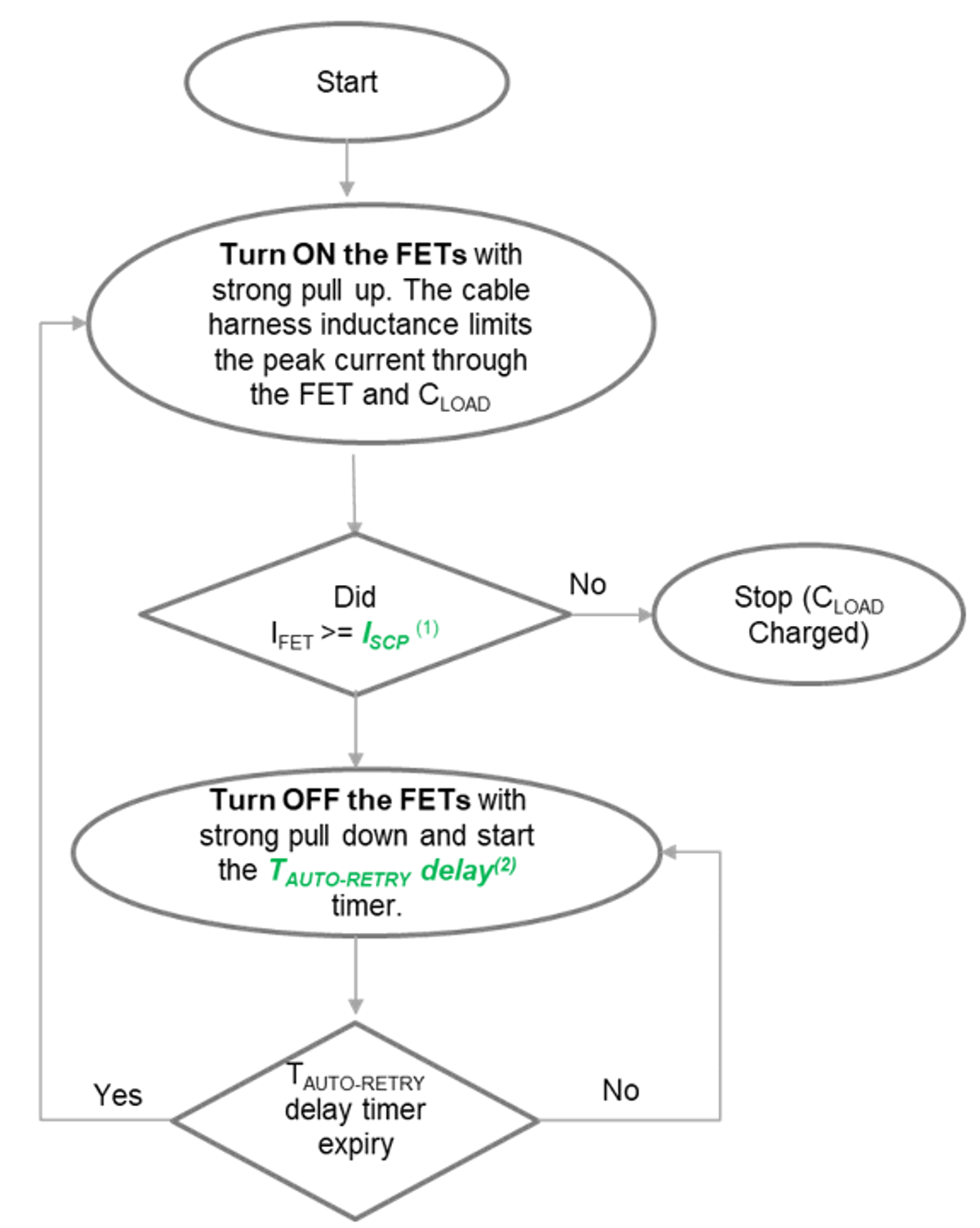
waveforms during startup.Figure 7 illustrates the control operation. As you can see, this approach has two variables, ISCP and TAUTO-RETRY, which need to be set for the high-side driver based on the input voltage (VIN), load capacitance and required charging time. A higher ISCP threshold or a shorter TAUTO-RETRY delay allow faster output charging, making the solution universal for any value of load capacitance.
 Figure 7 Flow chart of the PWM charging
control method.
Figure 7 Flow chart of the PWM charging
control method.This solution leverages the existing available real estate in a typical high-side driver system (the cable harness inductance and D1 diode) and creates an efficient charging method by operating the high-side MOSFETs in switching mode. Unlike traditional approaches, the proposed solution no longer depends on the FET SOA and does not require bulky precharge resistors, nor a precharge FET and driver. The solution uses the inherent short-circuit protection feature of the high-side driver and runs autonomously without any external control signals or complex algorithms.