SLYY211 October   2021 TMS320F2800132 , TMS320F2800133 , TMS320F2800135 , TMS320F2800137 , TMS320F2800152-Q1 , TMS320F2800153-Q1 , TMS320F2800154-Q1 , TMS320F2800155 , TMS320F2800155-Q1 , TMS320F2800156-Q1 , TMS320F2800157 , TMS320F2800157-Q1 , TMS320F280021 , TMS320F280021-Q1 , TMS320F280023 , TMS320F280023-Q1 , TMS320F280023C , TMS320F280025 , TMS320F280025-Q1 , TMS320F280025C , TMS320F280025C-Q1 , TMS320F280033 , TMS320F280034 , TMS320F280034-Q1 , TMS320F280036-Q1 , TMS320F280036C-Q1 , TMS320F280037 , TMS320F280037-Q1 , TMS320F280037C , TMS320F280037C-Q1 , TMS320F280038-Q1 , TMS320F280038C-Q1 , TMS320F280039 , TMS320F280039-Q1 , TMS320F280039C , TMS320F280039C-Q1 , TMS320F280040-Q1 , TMS320F280040C-Q1 , TMS320F280041 , TMS320F280041-Q1 , TMS320F280041C , TMS320F280041C-Q1 , TMS320F280045 , TMS320F280048-Q1 , TMS320F280048C-Q1 , TMS320F280049 , TMS320F280049-Q1 , TMS320F280049C , TMS320F280049C-Q1 , TMS320F28075 , TMS320F28075-Q1 , TMS320F28076 , TMS320F28374D , TMS320F28374S , TMS320F28375D , TMS320F28375S , TMS320F28375S-Q1 , TMS320F28376D , TMS320F28376S , TMS320F28377D , TMS320F28377D-EP , TMS320F28377D-Q1 , TMS320F28377S , TMS320F28377S-Q1 , TMS320F28378D , TMS320F28378S , TMS320F28379D , TMS320F28379D-Q1 , TMS320F28379S


  1. Message from the editors
  2. System Design
    1. 2.1 Control
      1. 2.1.1 Open loop versus closed loop
    2. 2.2 Feedback control
      1. 2.2.1 Error ratio
    3. 2.3 Dynamic systems
      1. 2.3.1 First order system
      2. 2.3.2 Second order system
    4. 2.4 System stability
      1. 2.4.1 Gain margin
      2. 2.4.2 Phase margin
    5. 2.5 Timing requirements
      1. 2.5.1 Peak/rise time
      2. 2.5.2 Settling time
      3. 2.5.3 Overshoot
      4. 2.5.4 Damping
      5. 2.5.5 Delay
    6. 2.6 Discrete Time Domain
    7. 2.7 Filters
      1. 2.7.1 Filter Types
      2. 2.7.2 Filter Orders
    8. 2.8 Notes
  3. Controllers
    1. 3.1 Linear PID
    2. 3.2 Linear PI
    3. 3.3 Nonlinear PID
    4. 3.4 2P2Z
    5. 3.5 3P3Z
    6. 3.6 Direct form controllers
      1. 3.6.1 DF11
      2. 3.6.2 DF13
      3. 3.6.3 DF22
      4. 3.6.4 DF23
    7. 3.7 Notes
  4. ADC
    1. 4.1 ADC definitions
    2. 4.2 ADC resolution
      1. 4.2.1 ADC resolution for unipolar
      2. 4.2.2 ADC resolution for differential signals
      3. 4.2.3 Resolution voltage vs. full-scale range
    3. 4.3 Quantization error of ADC
    4. 4.4 Total harmonic distortion (THD)
      1. 4.4.1 Total harmonic distortion (VRMS)
      2. 4.4.2 Total harmonic distortion (dBc)
    5. 4.5 AC signals
    6. 4.6 DC signals
    7. 4.7 Settling time and conversion accuracy
    8. 4.8 ADC system noise
    9. 4.9 Notes
  5. Comparator
    1. 5.1 Basic operation
    2. 5.2 Offset and hysteresis
    3. 5.3 Propagation delay
    4. 5.4 Notes
  6. Processing
    1. 6.1 Data representation
    2. 6.2 Central processing unit
      1. 6.2.1 CPU basics
      2. 6.2.2 CPU pipeline
      3. 6.2.3 Characteristics of a real-time processor
      4. 6.2.4 Signal chain
    3. 6.3 Memory
    4. 6.4 Direct memory access (DMA)
    5. 6.5 Interrupts
    6. 6.6 Co-processors and accelerators
    7. 6.7 Notes
  7. Encoders
    1. 7.1 Encoder definitions
    2. 7.2 Types of encoders
    3. 7.3 Description of encoders
      1. 7.3.1 Linear encoders
      2. 7.3.2 Rotary encoders
      3. 7.3.3 Position encoders
      4. 7.3.4 Optical encoders
    4. 7.4 Absolute Vs incremental encoders
      1. 7.4.1 Absolute rotary encoders
      2. 7.4.2 Incremental encoders
    5. 7.5 Notes
  8. Pulse width modulation (PWM)
    1. 8.1 PWM definitions
    2. 8.2 Duty cycle
    3. 8.3 Resolution
    4. 8.4 Deadband
    5. 8.5 Notes
  9. DAC
    1. 9.1 DAC definitions
    2. 9.2 DAC error
      1. 9.2.1 DAC offset error
      2. 9.2.2 DAC gain error
      3. 9.2.3 DAC zero-code error
      4. 9.2.4 DAC full-scale error
      5. 9.2.5 DAC differential non-linearity (DNL)
      6. 9.2.6 DAC integral non-linearity (INL)
      7. 9.2.7 DAC total unadjusted error (TUE)
    3. 9.3 DAC output considerations
      1. 9.3.1 DAC linear range
      2. 9.3.2 DAC settling time
      3. 9.3.3 DAC load regulation
    4. 9.4 Notes
  10. 10Mathematical models
    1. 10.1 Laplace transforms
    2. 10.2 Transfer function
    3. 10.3 Transient response
    4. 10.4 Frequency response
    5. 10.5 Z-domain
    6. 10.6 Notes
  11. 11Important Notice

Frequency response

If a steady state sine wave, u t =   u 0 sin ( ω t +   α ) is applied to a linear system denoted by G ( s ) , the linear system would respond at the same frequency with a certain phase and magnitude, giving output   y t =   y 0 sin ( ω t +   β ) . The amplitude is modified by y 0 u 0 and the phase is shifted by =   β - α   o r   < G ( j ω )

Bode plot basics

The frequency response for the magnitude or gain plot is the change in voltage gain as frequency changes. The change is specified on a Bode plot, a plot of frequency versus voltage gain in dB (decibles). Bode plots are usually plotted as semi-log plots with frequency on the x-axis, log scale, and gain on the y-axis, linear scale. The other half of the frequency response is the phase shift versus frequency and is plotted as frequency versus degree phase shift. Phase plots are usually plotted as semi-log plots with frequency on the x-axis, log scale, and phase shift on the y-axis, linear scale.

Definitions

Voltage gain in decibels

Equation 100. V o l t a g e   g a i n   d B = 20   l o g V O U T V I N
Power gain in decibels
Equation 101. P o w e r   g a i n   d B = 10   l o g P O U T P I N

Used for input or output power

Equation 102. P o w e r   m e a s u r e d   d B m = 10   l o g P o w e r   m e a s u r e d   ( W ) 1   m W
Table 10-3 Examples of common gain values and dB equivalent.
A (V/V) A (dB)
0.001 -60
0.01 -40
0.1 -20
1 0
10 20
100 40
1,000 60
10,000 80
100,000 100
1,000,000 120
10,000,000 140

Where

Roll-off rate is the decrease in gain with frequency

Decade is a tenfold increase or decrease in frequency (from 10 Hz to 100 Hz is one decade)

Octave is the doubling or halving of frequency (from 10 Hz to 20 Hz is one octave)

Bode plots: Poles
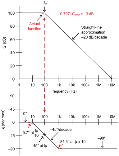
GUID-20210720-CA0I-RSS8-TVT8-3CCNTZM1BX56-low.gif Figure 10-1 Pole gain and phase.

Where

Pole location = f p (cutoff frequency)

Magnitude f <   f p = G D C (for example, 100 dB)

Magnitude f =   f p = -3 dB

Magnitude f >   f p = -20 dB/decade

Phase f =   f p = - 45 °

Phase 0.1   f p < f < 10   f p = - 45 ° /decade

Phase f > 10   f p = - 90 °

Phase f < 0.1   f p = 0 °

Pole (equations)

As a complex number

Equation 103. G V =   V O U T V I N =   G D C j f f p + 1

Magnitude

Equation 104. G V =   V O U T V I N =   G D C f f p 2 + 1

Phase Shift

Equation 105. θ =   - tan - 1 f f p

Magnitude in dB

Equation 106. G d B = 20 L o g ( G V )

Where

G V = voltage gain in V/V

G D B = voltage gain in decibels

G D C = the dc or low frequency voltage gain

f = frequency in Hz

f p = frequency at which the pole occurs

θ = phase shift of the signal from input to output

j = indicates imaginary number or - 1

Bode plot (zeros)

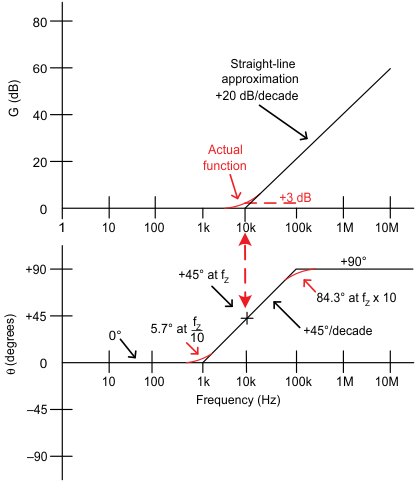
GUID-20210720-CA0I-QZ8J-V95M-BLLJHSWXXTB9-low.gif Figure 10-2 Zero gain and phase.

Where

Zero location = f z

Magnitude f <   f z = 0 dB

Magnitude f =   f z = +3 dB

Magnitude f >   f z = +20 dB/decade

Phase f =   f z = + 45 °

Phase 0.1   f z < f < 10   f z = + 45 ° /decade

Phase f > 10   f z = + 90 °

Phase f < 0.1   f z = 0 °

Zero (equations)

As a complex number

Equation 107. G V =   V O U T V I N = G D C j f f p + 1

Magnitude

Equation 108. G V =   V O U T V I N =   G D C f f z 2 + 1

Phase Shift

Equation 109. θ =   tan - 1 f z

Magnitude in dB

Equation 110. G d B = 20 L o g ( G V )

Where

G V = voltage gain in V/V

G D B = voltage gain in decibels

G D C = the dc or low frequency voltage gain

f = frequency in Hz

f z = frequency at which the zero occurs

θ = phase shift of the signal from input to output

j = indicates imaginary number or - 1