SLYY221 November 2023 ADC12DJ5200RF , ADS124S08 , ADS127L11 , AFE2256 , REF35 , REF70 , TPS62912 , TPS62913 , TPS7A94 , TPSM82912 , TPSM82913 , UCC5880-Q1
- 1
- Overview
- At a glance
- Why high voltage?
- Optimizing wide-bandgap FET performance with component innovations
- Selecting the right gate drivers
- Selecting the right controllers
- Maximizing power density with topology innovations
- Achieving extreme efficiency targets with system-level innovation
- Addressing EMI challenges
- Conclusion
- Additional resources
Selecting the right gate drivers
Because of their electrical properties and the performance they enable, switching to wide band-gap technologies requires a thoughtful approach and careful companion component selection, presenting a completely different set of challenges than designing with silicon. To further minimize switching losses, wide band-gap FETs need an appropriate gate driver capable of rapidly charging and discharging the gate capacitance, since traditional silicon MOSFET gate drivers may not offer proper voltage regulation or be able to handle the high common-mode voltage transient in a wide band-gap design.
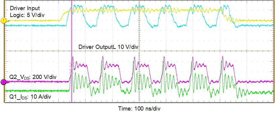
As shown in Figure 2, when a switching event occurs, the voltage change on the switching node will generate a current flow through the parasitic capacitance of the driver. If the driver does not have enough common-mode transient immunity (CMTI), the common-mode current could cause a gate-driver malfunction, as shown in Figure 3.
 Figure 2 Common-mode current caused by
a switching event.
 Figure 3 Gate-driver CMTI failure
example.
Figure 3 Gate-driver CMTI failure
example.To address gate-driver challenges and CMTI concerns, engineers can use new gate drivers with a Miller clamp, a high CMTI rating and adjustable slew-rate features to avoid shoot-through or a gate-driver malfunction. TI’s UCC5880-Q1 reinforced isolated gate driver has as much as 20 A of real-time variable gate-drive strength, a feature that enables you to increase power density and reduce system design complexity and cost while achieving your safety and performance goals. TI’s 300-kW DC/AC High-Power, High-Performance Automotive SiC Traction Inverter Reference Design demonstrates how to balance efficiency and the challenges discussed here by adjusting driving speeds under different load conditions.
Faster switching means lower switching losses, but it can also lead to unwanted voltage ringing and common-mode noise issues. Figure 4 shows a GaN FET with a discrete gate driver. There is not only parasitic inductance of the two devices themselves, but also the printed circuit board (PCB) trace inductance of the connection copper. The total inductance on the driving loop will slow the GaN FET VDS transition, therefore limiting the switching losses that the GaN FET can reduce. This is why a TI GaN FET such as the LMG3526R030 (see Figure 5) integrates a gate driver into the same package. With the gate driver integrated, there will be no PCB inductance (Lg_pcb and Ls_pcb). Also, the Kelvin source connection is made for the gate-drive loop (minimizing Lcs); therefore, the TI GaN FET can switch at a high transient voltage, which will minimize switching losses.
 Figure 4 A GaN FET with a discrete gate
driver and parasitic inductance on the loop.
 Figure 5 Simplified LMG3526R030 block
diagram.