SLYY221 November 2023 ADC12DJ5200RF , ADS124S08 , ADS127L11 , AFE2256 , REF35 , REF70 , TPS62912 , TPS62913 , TPS7A94 , TPSM82912 , TPSM82913 , UCC5880-Q1
- 1
- Overview
- At a glance
- Why high voltage?
- Optimizing wide-bandgap FET performance with component innovations
- Selecting the right gate drivers
- Selecting the right controllers
- Maximizing power density with topology innovations
- Achieving extreme efficiency targets with system-level innovation
- Addressing EMI challenges
- Conclusion
- Additional resources
Addressing EMI challenges
Engineers can address EMI filter design challenges by splitting the PFC inductor into two elements: one with the higher-inductance inductor (Lg) connected to an AC source, and the lower-inductance inductor (Lb) in series with a capacitor and placed in parallel with the power stage, as shown in Figure 13. The idea of splitting inductor setup is to allow the large AC ripple current to flow through the series inductor and capacitor (lower total impedance) and to minimize the current ripple on Lb (higher impedance) and the AC source. Therefore, EMI filter design becomes easier, as the differential mode noise is lower.
 Figure 13 A modified totem-pole
bridgeless PFC circuit.
Figure 13 A modified totem-pole
bridgeless PFC circuit.Although the modified soft-switching CRM PFC does allow you to overcome EMI filter design challenges, the CRM PFC itself requires additional sensing and control efforts to determine PFC active switch turnon timing in order to ensure soft switching. One option is to add current-sensing devices such as a current transformer to detect the zero current point, which allows you to then calculate active FET turnon timing based on the FET Coss. Propagation delay in sensing and control systems and component tolerance will result in active FET turnon timing errors. Since this control scheme requires cycle-by-cycle sensing and control, you should expect higher MCU resource usage.
An alternative way is to calculate the required FET’s on- and off-time based on the input and output voltage-sensing results, along with the PFC inductance and FET Coss. You can then use the FET drain-to-source voltage sensing to determine whether you’ve achieved soft switching. If the drain-to-source voltage doesn’t go negative before the gate signal goes high, it means that the FET is in hard switching.
Take the FETs shown in Figure 13 as an example, where extending the HFFET_HS on-time allows more negative current to discharge HFFET_LS Coss in order to achieve soft switching. If the drain-to-source voltage goes negative before the gate signal goes high, it means that the FET is already soft switching. Reducing the on-time of HFFET_HS will minimize the root-mean-square current for better efficiency. This way, the FET on-time is no longer updated every cycle but is only adjusting when soft switching isn’t occurring, which saves a lot on MCU resource usage.
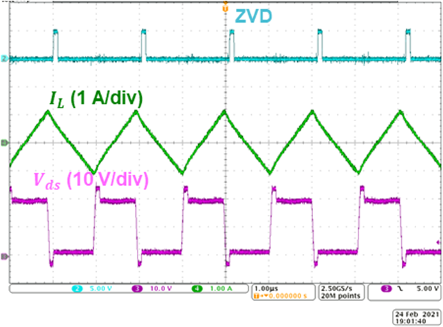
Integrating the required soft-switching sensing circuit with the FET could further simplify the system. As shown in Figure 5, the LMG3526R030 device integrates a GaN FET, driver, protections and FET drain-to-source voltage sensing into one package. Whenever the GaN FET is in third-quadrant conduction before channel conduction, the LMG3526R030 sends out a zero-voltage detection pulse as an indication of soft switching.
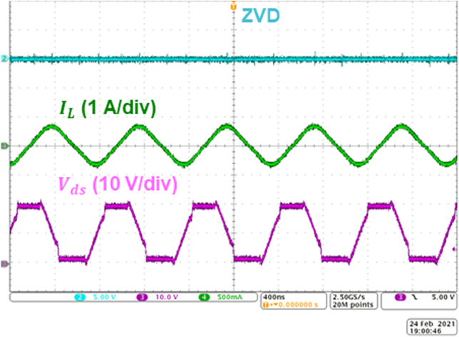
Figure 14 shows example waveforms of the LMG3526R030 with and without third-quadrant conduction.

 Figure 14 Waveform of the LMG3526R030
with (upper one) and without third-quadrant conduction.
Figure 14 Waveform of the LMG3526R030
with (upper one) and without third-quadrant conduction.Using the zero-voltage detection feature in LMG3526R030, The Variable-Frequency, ZVS, 5-kW, GaN-Based, Two-Phase Totem-Pole PFC Reference Design has demonstrated over 99.1% peak efficiency by combining component, topology and control system innovations.