SNAA409 April 2024 LMX2594
This brief covers on how to interface RF synthesizers with Microcontroller. In general, USB2ANY is used for this interfacing. But USB2ANY has some limitations namely low frequency SPI write and wait-time between two SPI writes in burst mode. For some applications, this low frequency SPI and wait-time might not be acceptable. For this brief, register writes present in the script shared is applicable for LMX2594 Synthesizer. In general, same approach can be used for all RF synthesizers.
Components Required:
- LMX2594EVM
- USB2ANY with 10-pin JTAG cable
- TICS Pro GUI (Downloadable from ti.com)
- Code Composer Studio (CCS) – Latest Version downloadable from ti.com
- MSP430W are (Downloadable from ti.com)
- LMX2594_MSP430 Script (extractable from TI Drive)
- Programmable DC Power Supply (Output should be capable to give 3.3V at 0.6A current limit)
- 40GHz SMA Cable (Optional)
- Spectrum Analyzer/Phase Noise Analyzer (Optional)
- 100MHz Wenzel/Clean reference input source (optional if crystal is mounted on the LMX2594 EVM)
Test Setup:
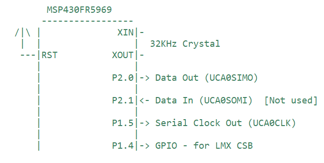
Connect the MSP430FRxxxx EVM to the LMX2594EVM through the JTAG connection pins as per the figure below:
 Figure 1 MSP430FR5969 Pins on EVM
The USB2ANY 10-pin adapter cable pinout is shown below for reference. The connections are summarized in the following table:
| MCU Pins | JTAG Adapter Pinout | LMX2594EVM Header |
|---|---|---|
| P1.4 GPIO | SPI_CS, Pin 2 | Right Row, Header 1 |
| GND | GND, Pin 6 | Right Row, Header 3 |
| P1.5 GPIO | SPI_SCLK, Pin 8 | Right Row, Header 4 |
| P2.0 GPIO | SPI_SIMO, Pin 4 | Right Row, Header 2 |
 Figure 2 10-Pin Cable Pinouts
| Schematic Pin Number | Cable Pin Number | Signals Available |
|---|---|---|
| J4-10 | 1 | GPIO7, PWM0, INT2, OW2, OW5 |
| J4-9 | 2 | GPIO6, PWM1, RFFE:SCLK, SPI:CS, INT1, μWIRE:CS, OW1 |
| J4-8 | 3 | GPIO5, SPI:SOMI, UART:RXD, μWIRE:SOMI |
| J4-7 | 4 | GPIO4, SPI:SIMO, UART:TXD, μWIRE:SOMI |
| J4-6 | 5 | 3.3VEXT |
| J4-5 | 6 | GND |
| J4-4 | 7 | GPIO3, PWM2, RFFE:SDATA, INT0 |
| J4-3 | 8 | GPIO2, ES:DOUT, SPI:SCLK, μWIRE:SCLK |
Procedure:
- Connect the USB2ANY to a host PC/laptop with the 10-pin adapter cable connected to the LMX2594EVM.
- Supply power to the LMX2594EVM with the output set to 3.3V and 0.6A current limit.
- If a 100MHz crystal is not mounted on the EVM, then use a 100MHz Wenzel to give a reference input to the EVM through the OSCINP pin. A signal generator set to 10dBm at 100MHz also works here.
- With the TICS Pro GUI installed, select the LMX2594 device under the PLL+VCO section. Set the desired output frequency in full assist mode as per the EVM instructions given here.
- In the “Raw Registers” section, record the following register values:Table 3 LMX2594 Register Mapping
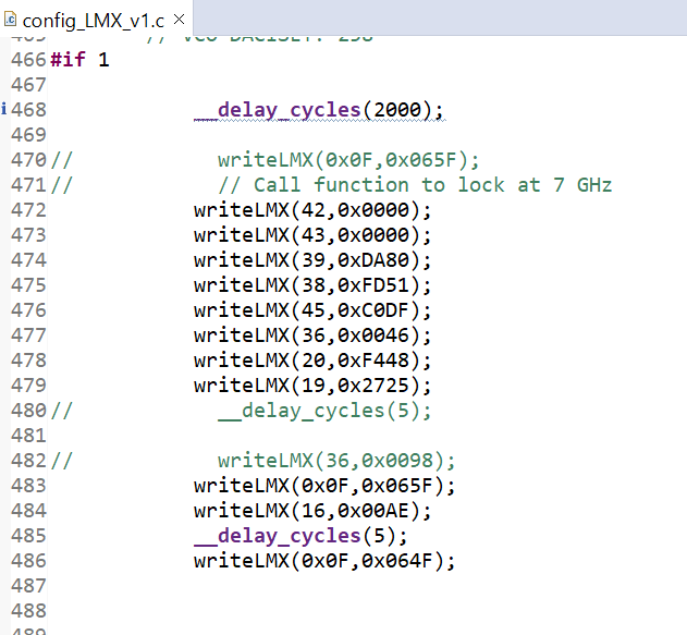
Register Name Corresponding Function R36 N Divider R38 Denominator R39 R42 Numerator R43 R45 OUT_ISET R20 VCO_SEL_FORCE R19 VCO_CAPCTRL R16 VCO_DACISET - Open CCS and enter the recorded values of the register into the LMX_MSP430 script shared via TI Drive as shown below. You can use the shared excel sheet on TI Drive to quickly copy and paste the writeLMX commands:
 Figure 3 Sequence of Register Writes for Switching Between Two Frequencies.
 - Remove the USB2ANY connection from the laptop/PC and connect the MSP430 to the LMX2594EVM as per the Test Setup section given in this document.
- Run the CCS script and check the device LED to verify the lock state of the PLL Synthesizer to the desired output frequency.