SNAS669E September 2015 – April 2018 LMK03318
PRODUCTION DATA.
- 1 Features
- 2 Applications
- 3 Description
- 4 Revision History
- 5 Description (continued)
- 6 Device Comparison Table
- 7 Pin Configuration and Functions
-
8 Specifications
- 8.1 Absolute Maximum Ratings
- 8.2 ESD Ratings
- 8.3 Recommended Operating Conditions
- 8.4 Thermal Information
- 8.5 Thermal Information
- 8.6 Electrical Characteristics - Power Supply
- 8.7 Pullable Crystal Characteristics (SECREF_P, SECREF_N)
- 8.8 Non-Pullable Crystal Characteristics (SECREF_P, SECREF_N)
- 8.9 Clock Input Characteristics (PRIREF_P/PRIREF_N, SECREF_P/SECREF_N)
- 8.10 VCO Characteristics
- 8.11 PLL Characteristics
- 8.12 1.8-V LVCMOS Output Characteristics (OUT[7:0])
- 8.13 LVCMOS Output Characteristics (STATUS[1:0])
- 8.14 Open-Drain Output Characteristics (STATUS[1:0])
- 8.15 AC-LVPECL Output Characteristics
- 8.16 AC-LVDS Output Characteristics
- 8.17 AC-CML Output Characteristics
- 8.18 HCSL Output Characteristics
- 8.19 Power-On Reset Characteristics
- 8.20 2-Level Logic Input Characteristics (HW_SW_CTRL, PDN, GPIO[5:0])
- 8.21 3-Level Logic Input Characteristics (REFSEL, GPIO[3:1])
- 8.22 Analog Input Characteristics (GPIO[5])
- 8.23 I2C-Compatible Interface Characteristics (SDA, SCL)
- 8.24 Typical 156.25-MHz Closed-Loop Output Phase Noise Characteristics
- 8.25 Typical 161.1328125-MHz Closed-Loop Output Phase Noise Characteristics
- 8.26 Closed-Loop Output Jitter Characteristics
- 8.27 PCIe Clock Output Jitter
- 8.28 Typical Power Supply Noise Rejection Characteristics
- 8.29 Typical Power-Supply Noise Rejection Characteristics
- 8.30 Typical Closed-Loop Output Spur Characteristics
- 8.31 Typical Characteristics
- 9 Parameter Measurement Information
-
10Detailed Description
- 10.1 Overview
- 10.2 Functional Block Diagram
- 10.3 Feature Description
- 10.4
Device Functional Modes
- 10.4.1 Smart Input MUX
- 10.4.2 Universal Input Buffer (PRI_REF, SEC_REF)
- 10.4.3 Crystal Input Interface (SEC_REF)
- 10.4.4 Reference Doubler
- 10.4.5 Reference Divider (R)
- 10.4.6 Input Divider (M)
- 10.4.7 Feedback Divider (N)
- 10.4.8 Phase Frequency Detector (PFD)
- 10.4.9 Charge Pump
- 10.4.10 Loop Filter
- 10.4.11 VCO Calibration
- 10.4.12 Fractional Circuitry
- 10.4.13 Post Divider
- 10.4.14 High-Speed Output MUX
- 10.4.15 High-Speed Output Divider
- 10.4.16 High-Speed Clock Outputs
- 10.4.17 Output Synchronization
- 10.4.18 Status Outputs
- 10.5 Programming
- 10.6
Register Maps
- 10.6.1 VNDRID_BY1 Register; R0
- 10.6.2 VNDRID_BY0 Register; R1
- 10.6.3 PRODID Register; R2
- 10.6.4 REVID Register; R3
- 10.6.5 PARTID Register; R4
- 10.6.6 PINMODE_SW Register; R8
- 10.6.7 PINMODE_HW Register; R9
- 10.6.8 SLAVEADR Register; R10
- 10.6.9 EEREV Register; R11
- 10.6.10 DEV_CTL Register; R12
- 10.6.11 INT_LIVE Register; R13
- 10.6.12 INT_MASK Register; R14
- 10.6.13 INT_FLAG_POL Register; R15
- 10.6.14 INT_FLAG Register; R16
- 10.6.15 INTCTL Register; R17
- 10.6.16 OSCCTL2 Register; R18
- 10.6.17 STATCTL Register; R19
- 10.6.18 MUTELVL1 Register; R20
- 10.6.19 MUTELVL2 Register; R21
- 10.6.20 OUT_MUTE Register; R22
- 10.6.21 STATUS_MUTE Register; R23
- 10.6.22 DYN_DLY Register; R24
- 10.6.23 REFDETCTL Register; R25
- 10.6.24 STAT0_INT Register; R27
- 10.6.25 STAT1 Register; R28
- 10.6.26 OSCCTL1 Register; R29
- 10.6.27 PWDN Register; R30
- 10.6.28 OUTCTL_0 Register; R31
- 10.6.29 OUTCTL_1 Register; R32
- 10.6.30 OUTDIV_0_1 Register; R33
- 10.6.31 OUTCTL_2 Register; R34
- 10.6.32 OUTCTL_3 Register; R35
- 10.6.33 OUTDIV_2_3 Register; R36
- 10.6.34 OUTCTL_4 Register; R37
- 10.6.35 OUTDIV_4 Register; R38
- 10.6.36 OUTCTL_5 Register; R39
- 10.6.37 OUTDIV_5 Register; R40
- 10.6.38 OUTCTL_6 Register; R41
- 10.6.39 OUTDIV_6 Register; R42
- 10.6.40 OUTCTL_7 Register; R43
- 10.6.41 OUTDIV_7 Register; R44
- 10.6.42 CMOSDIVCTRL Register; R45
- 10.6.43 CMOSDIV0 Register; R46
- 10.6.44 STATUS_SLEW Register; R49
- 10.6.45 IPCLKSEL Register; R50
- 10.6.46 IPCLKCTL Register; R51
- 10.6.47 PLL_RDIV Register; R52
- 10.6.48 PLL_MDIV Register; R53
- 10.6.49 PLL_CTRL0 Register; R56
- 10.6.50 PLL_CTRL1 Register; R57
- 10.6.51 PLL_NDIV_BY1 Register; R58
- 10.6.52 PLL_NDIV_BY0 Register; R59
- 10.6.53 PLL_FRACNUM_BY2 Register; R60
- 10.6.54 PLL_FRACNUM_BY1 Register; R61
- 10.6.55 PLL_FRACNUM_BY0 Register; R62
- 10.6.56 PLL_FRACDEN_BY2 Register; R63
- 10.6.57 PLL_FRACDEN_BY1 Register; R64
- 10.6.58 PLL_FRACDEN_BY0 Register; R65
- 10.6.59 PLL_MASHCTRL Register; R66
- 10.6.60 PLL_LF_R2 Register; R67
- 10.6.61 PLL_LF_C1 Register; R68
- 10.6.62 PLL_LF_R3 Register; R69
- 10.6.63 PLL_LF_C3 Register; R70
- 10.6.64 SEC_CTRL Register; R72
- 10.6.65 XO_MARGINING Register; R86
- 10.6.66 XO_OFFSET_GPIO5_STEP_1_BY1 Register; R88
- 10.6.67 XO_OFFSET_GPIO5_STEP_1_BY0 Register; R89
- 10.6.68 XO_OFFSET_GPIO5_STEP_2_BY1 Register; R90
- 10.6.69 XO_OFFSET_GPIO5_STEP_2_BY0 Register; R91
- 10.6.70 XO_OFFSET_GPIO5_STEP_3_BY1 Register; R92
- 10.6.71 XO_OFFSET_GPIO5_STEP_3_BY0 Register; R93
- 10.6.72 XO_OFFSET_GPIO5_STEP_4_BY1 Register; R94
- 10.6.73 XO_OFFSET_GPIO5_STEP_4_BY0 Register; R95
- 10.6.74 XO_OFFSET_GPIO5_STEP_5_BY1 Register; R96
- 10.6.75 XO_OFFSET_GPIO5_STEP_5_BY0 Register; R97
- 10.6.76 XO_OFFSET_GPIO5_STEP_6_BY1 Register; R98
- 10.6.77 XO_OFFSET_GPIO5_STEP_6_BY0 Register; R99
- 10.6.78 XO_OFFSET_GPIO5_STEP_7_BY1 Register; R100
- 10.6.79 XO_OFFSET_GPIO5_STEP_7_BY0 Register; R101
- 10.6.80 XO_OFFSET_GPIO5_STEP_8_BY1 Register; R102
- 10.6.81 XO_OFFSET_GPIO5_STEP_8_BY0 Register; R103
- 10.6.82 XO_OFFSET_SW_BY1 Register; R104
- 10.6.83 XO_OFFSET_SW_BY0 Register; R105
- 10.6.84 PLL_CTRL2 Register; R117
- 10.6.85 PLL_CTRL3 Register; R118
- 10.6.86 PLL_CALCTRL0 Register; R119
- 10.6.87 PLL_CALCTRL1 Register; R120
- 10.6.88 NVMCNT Register; R136
- 10.6.89 NVMCTL Register; R137
- 10.6.90 NVMLCRC Register; R138
- 10.6.91 MEMADR_BY1 Register; R139
- 10.6.92 MEMADR_BY0 Register; R140
- 10.6.93 NVMDAT Register; R141
- 10.6.94 RAMDAT Register; R142
- 10.6.95 ROMDAT Register; R143
- 10.6.96 NVMUNLK Register; R144
- 10.6.97 REGCOMMIT_PAGE Register; R145
- 10.6.98 XOCAPCTRL_BY1 Register; R199
- 10.6.99 XOCAPCTRL_BY0 Register; R200
- 10.6.100 EEPROM Map
- 11Application and Implementation
- 12Power Supply Recommendations
- 13Layout
- 14Device and Documentation Support
- 15Mechanical, Packaging, and Orderable Information
10.5.1 I2C Serial Interface
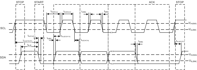
The I2C port on the LMK03318 works as a slave device and supports both the 100 kHz standard mode and 400 kHz fast-mode operations. Fast mode imposes a glitch tolerance requirement on the control signals. Therefore, the input receivers ignore pulses of less than 50-ns duration. The I2C timing is given in I2C-Compatible Interface Characteristics (SDA, SCL) I2C-Compatible Interface Characteristics (SDA, SCL). The timing diagram is given in Figure 71.
 Figure 71. I2C Timing Diagram
In an I2C bus system, the LMK03318 acts as a slave device and is connected to the serial bus (data bus SDA and clock bus SCL). These are accessed through a 7-bit slave address transmitted as part of an I2C packet. Only the device with a matching slave address responds to subsequent I2C commands. In soft pin mode, the LMK03318 allows up to three unique slave devices to occupy the I2C bus based on the pin strapping of GPIO1 (tied to VDD_DIG, GND or VIM). The device slave address is 10100xx (the two LSBs are determined by the GPIO1 pin).
NOTE
The PDN pin of LMK03318 should be high before any I2C communication on the bus. The first I2C transaction after power cycling LMK03318 should be ignored.
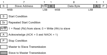
During the data transfer through the I2C interface, one clock pulse is generated for each data bit transferred. The data on the SDA line must be stable during the high period of the clock. The high or low state of the data line can change only when the clock signal on the SCL line is low. The start data transfer condition is characterized by a high-to-low transition on the SDA line while SCL is high. The stop data transfer condition is characterized by a low-to-high transition on the SDA line while SCL is high. The start and stop conditions are always initiated by the master. Every byte on the SDA line must be eight bits long. Each byte must be followed by an acknowledge bit and bytes are sent MSB first. The I2C register structure of the LMK03318 is shown in Figure 72.
 Figure 72. I2C Register Structure
The acknowledge bit (A) or non-acknowledge bit (A’) is the 9th bit attached to any 8-bit data byte and is always generated by the receiver to inform the transmitter that the byte has been received (when A = 0) or not (when A’ = 0). A = 0 is done by pulling the SDA line low during the 9th clock pulse and A’ = 0 is done by leaving the SDA line high during the 9th clock pulse.
The I2C master initiates the data transfer by asserting a start condition which initiates a response from all slave devices connected to the serial bus. Based on the 8-bit address byte sent by the master over the SDA line (consisting of the 7-bit slave address (MSB first) and an R/W’ bit), the device whose address corresponds to the transmitted address responds by sending an acknowledge bit. All other devices on the bus remain idle while the selected device waits for data transfer with the master.
After the data transfer has occurred, stop conditions are established. In write mode, the master asserts a stop condition to end data transfer during the 10th clock pulse following the acknowledge bit for the last data byte from the slave. In read mode, the master receives the last data byte from the slave but does not pull SDA low during the 9th clock pulse. This is known as a non-acknowledge bit. By receiving the non-acknowledge bit, the slave knows the data transfer is finished and enters the idle mode. The master then takes the data line low during the low period before the 10th clock pulse, and high during the 10th clock pulse to assert a stop condition. A generic transation is shown in Figure 73.
 Figure 73. Generic Programming Sequence
The LMK03318 I2C interface supports “Block Register Write/Read”, “Read/Write SRAM”, and “Read/Write EEPROM” operations. For “Block Register Write/Read” operations, the I2C master can individually access addressed registers that are made of an 8-bit data byte. The offset of the indexed register is encoded in R10 and part of the EEPROM, as described in Table 9 below. To change the most significant 5 bits of the I2C slave address from its default value, the EEPROM byte 11 can be re-written with the desired value and R10 provides a read-back of the new slave address.
Table 9. I2C Slave Address
| Operating Mode | R10.7 | R10.6 | R10.5 | R10.4 | R10.3 | R10.2 | R10.1 |
|---|---|---|---|---|---|---|---|
| Hard pin | 1 | 0 | 1 | 0 | 0 | 0 | 0 |
| Soft pin | 1 | 0 | 1 | 0 | 0 | Controlled by GPIO1 state. | |
| GPIO1 | R10[2-1] | ||||||
| 0 | 0x0 | ||||||
| VIM | 0x1 | ||||||
| 1 | 0x3 | ||||||