SNAS696C March   2017  – April 2019 LMX2594

PRODUCTION DATA.  

  1. Features
  2. Applications
  3. Description
    1.     Device Images
      1.      Simplified Schematic
  4. Revision History
  5. Pin Configuration and Functions
    1.     Pin Functions
  6. Specifications
    1. 6.1 Absolute Maximum Ratings
    2. 6.2 ESD Ratings
    3. 6.3 Recommended Operating Conditions
    4. 6.4 Thermal Information
    5. 6.5 Electrical Characteristics
    6. 6.6 Timing Requirements
    7. 6.7 Typical Characteristics
  7. Detailed Description
    1. 7.1 Overview
    2. 7.2 Functional Block Diagram
    3. 7.3 Feature Description
      1. 7.3.1  Reference Oscillator Input
      2. 7.3.2  Reference Path
        1. 7.3.2.1 OSCin Doubler (OSC_2X)
        2. 7.3.2.2 Pre-R Divider (PLL_R_PRE)
        3. 7.3.2.3 Programmable Multiplier (MULT)
        4. 7.3.2.4 Post-R Divider (PLL_R)
        5. 7.3.2.5 State Machine Clock
      3. 7.3.3  PLL Phase Detector and Charge Pump
      4. 7.3.4  N-Divider and Fractional Circuitry
      5. 7.3.5  MUXout Pin
        1. 7.3.5.1 Lock Detect
        2. 7.3.5.2 Readback
      6. 7.3.6  VCO (Voltage-Controlled Oscillator)
        1. 7.3.6.1 VCO Calibration
        2. 7.3.6.2 Determining the VCO Gain
      7. 7.3.7  Channel Divider
      8. 7.3.8  Output Buffer
      9. 7.3.9  Power-Down Modes
      10. 7.3.10 Phase Synchronization
        1. 7.3.10.1 General Concept
        2. 7.3.10.2 Categories of Applications for SYNC
        3. 7.3.10.3 Procedure for Using SYNC
        4. 7.3.10.4 SYNC Input Pin
      11. 7.3.11 Phase Adjust
      12. 7.3.12 Fine Adjustments for Phase Adjust and Phase SYNC
      13. 7.3.13 Ramping Function
        1. 7.3.13.1 Manual Pin Ramping
          1. 7.3.13.1.1 Manual Pin Ramping Example
        2. 7.3.13.2 Automatic Ramping
          1. 7.3.13.2.1 Automatic Ramping Example (Triangle Wave)
      14. 7.3.14 SYSREF
        1. 7.3.14.1 Programmable Fields
        2. 7.3.14.2 Input and Output Pin Formats
          1. 7.3.14.2.1 Input Format for SYNC and SysRefReq Pins
          2. 7.3.14.2.2 SYSREF Output Format
        3. 7.3.14.3 Examples
        4. 7.3.14.4 SYSREF Procedure
      15. 7.3.15 SysRefReq Pin
    4. 7.4 Device Functional Modes
    5. 7.5 Programming
      1. 7.5.1 Recommended Initial Power-Up Sequence
      2. 7.5.2 Recommended Sequence for Changing Frequencies
      3. 7.5.3 General Programming Requirements
    6. 7.6 Register Maps
      1. 7.6.1  General Registers R0, R1, & R7
        1. Table 24. Field Descriptions
      2. 7.6.2  Input Path Registers
        1. Table 25. Field Descriptions
      3. 7.6.3  Charge Pump Registers (R13, R14)
        1. Table 26. Field Descriptions
      4. 7.6.4  VCO Calibration Registers
        1. Table 27. Field Descriptions
      5. 7.6.5  N Divider, MASH, and Output Registers
        1. Table 28. Field Descriptions
      6. 7.6.6  SYNC and SysRefReq Input Pin Register
        1. Table 29. Field Descriptions
      7. 7.6.7  Lock Detect Registers
        1. Table 30. Field Descriptions
      8. 7.6.8  MASH_RESET
        1. Table 31. Field Descriptions
      9. 7.6.9  SysREF Registers
        1. Table 32. Field Descriptions
      10. 7.6.10 CHANNEL Divider Registers
        1. Table 33. Field Descriptions
      11. 7.6.11 Ramping and Calibration Fields
        1. Table 34. Field Descriptions
      12. 7.6.12 Ramping Registers
        1. 7.6.12.1 Ramp Limits
          1. Table 35. Field Descriptions
        2. 7.6.12.2 Ramping Triggers, Burst Mode, and RAMP0_RST
          1. Table 36. Field Descriptions
        3. 7.6.12.3 Ramping Configuration
          1. Table 37. Field Descriptions
      13. 7.6.13 Readback Registers
        1. Table 38. Field Descriptions
  8. Application and Implementation
    1. 8.1 Application Information
      1. 8.1.1 OSCin Configuration
      2. 8.1.2 OSCin Slew Rate
      3. 8.1.3 RF Output Buffer Power Control
      4. 8.1.4 RF Output Buffer Pullup
    2. 8.2 Typical Application
      1. 8.2.1 Design Requirements
      2. 8.2.2 Detailed Design Procedure
      3. 8.2.3 Application Curve
  9. Power Supply Recommendations
  10. 10Layout
    1. 10.1 Layout Guidelines
    2. 10.2 Layout Example
  11. 11Device and Documentation Support
    1. 11.1 Device Support
      1. 11.1.1 Third-Party Products Disclaimer
      2. 11.1.2 Development Support
    2. 11.2 Documentation Support
      1. 11.2.1 Related Documentation
    3. 11.3 Receiving Notification of Documentation Updates
    4. 11.4 Community Resources
    5. 11.5 Trademarks
    6. 11.6 Electrostatic Discharge Caution
    7. 11.7 Glossary
  12. 12Mechanical, Packaging, and Orderable Information

SYSREF

The LMX2594 can generate a SYSREF output signal that is synchronized to fOUT with a programmable delay. This output can be a single pulse, series of pulses, or a continuous stream of pulses. To use the SYSREF capability, the PLL must first be placed in SYNC mode with VCO_PHASE_SYNC = 1.

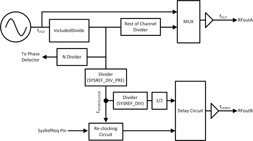
LMX2594 SYSREF_diagram_snas696.gifFigure 30. SYSREF Setup

As Figure 30 shows, the SYSREF feature uses IncludedDivide and SYSREF_DIV_PRE divider to generate fINTERPOLATOR. This frequency is used for reclocking of the rising and falling edges at the SysRefReq pin. In master mode, the fINTERPOLATOR is further divided by 2 × SYSREF_DIV to generate finite series or continuous stream of pulses.

Table 18. SYSREF Setup

PARAMETER MIN TYP MAX UNIT
fVCO 7.5 15 GHz
fINTERPOLATOR 0.8 1.5 GHz
IncludedDivide 4 or 6
SYSREF_DIV_PRE 1, 2, or 4
SYSREF_DIV 4,6,8, ... , 4098
fINTERPOLATOR fINTERPOLATOR = fVCO / (IncludedDivide × SYSREF_DIV_PRE)
fSYSREF fSYSREF = fINTERPOLATOR / (2 × SYSREF_DIV)
Delay step size 9 ps
Pulses for pulsed mode (SYSREF_PULSE_CNT) 0 15 n/a

The delay can be programmed using the JESD_DAC1_CTRL, JESD_DAC2_CTRL, JESD_DAC3_CTRL, and JESD_DAC4_CTRL words. By concatenating these words into a larger word called "SYSREFPHASESHIFT", the relative delay can be found. The sum of these words should always be 63.

Table 19. SysRef Delay

SYSREFPHASESHIFT DELAY JESD_DAC1 JESD_DAC2 JESD_DAC3 JESD_DAC4
0 Minimum 36 27 0 0
... 0 0
36 0 63 0 0
37 62 1 0 0
...
99 0 0 63 0
100 0 0 62 1
...
161 0 0 1 62
162 0 0 0 63
163 1 0 0 62
225 63 0 0 0
226 62 1 0 0
247 Maximum 41 22 0 0
> 247 Invalid Invalid Invalid Invalid Invalid