SNLU292A November   2020  – March 2022 DP83TC812R-Q1 , DP83TC812S-Q1 , DP83TC814R-Q1 , DP83TC814S-Q1


  1. 1Revision History
    1.     Trademarks
  2. 2Introduction
    1. 2.1 Key Features
    2. 2.2 Operation – Quick Setup
      1. 2.2.1 Onboard Power Supply Operation
      2. 2.2.2 SMI Connection and Communication
        1. 2.2.2.1 On-board MSP Connection
        2. 2.2.2.2 Downloading USB2MDIO for SMI
        3. 2.2.2.3 SMI Interface
      3. 2.2.3 Master and Slave Mode Selection – DP83TC812
      4. 2.2.4 Wake Selection – DP83TC812
      5. 2.2.5 LED Indication
  3. 3Board Setup Details
    1. 3.1 Block Diagram
    2. 3.2 Configuration Options
      1. 3.2.1 Clock Configuration
  4. 4Definitions
  5. 5Schematics
    1. 5.1 Main Block Schematic
    2. 5.2 DP83867 Schematic
    3. 5.3 Power Schematic
    4. 5.4 AFE Schematic
    5. 5.5 Comms Schematic
    6. 5.6 Hardware Schematic
  6. 6Layout

Wake Selection – DP83TC812

  • Place shunt in PU position at WAKE header shown to pull wake pin of DP83TC812.
  • Place shunt in GND position at WAKE header shown to pull down wake pin of DP83TC812.

Figure 2-7 shows jumper in PU position on header.
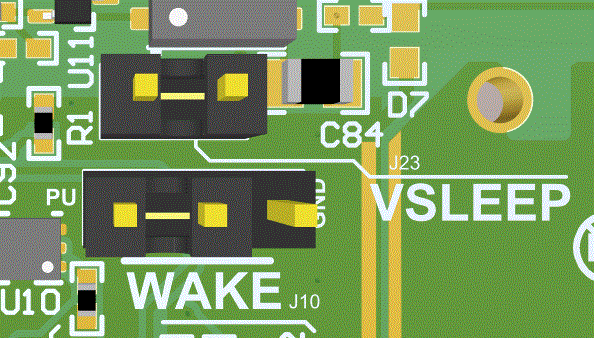
GUID-AE523515-3FAB-4A6D-932E-104080069B7C-low.gifFigure 2-7 Wake pin in pulled up position