SNLU297 May 2021 DS320PR810
- Trademarks
- 1Introduction
-
2Description
- 2.1 DS320PR810 5-Level I/O Control Inputs
- 2.2 DS320PR810 Modes of Operation
- 2.3 DS320PR810 SMBus or I2C Register Control Interface
- 2.4 DS320PR810 Equalization Control
- 2.5 DS320PR810 RX Detect State Machine
- 2.6 DS320PR810 DC Gain Control
- 2.7 DS320PR810 EVM Global Controls
- 2.8 DS320PR810EVM Downstream Devices Control
- 2.9 DS320PR810EVM Upstream Devices Control
- 2.10 Quick-Start Guide (Pin Mode)
- 2.11 Quick-Start Guide (SMBus Slave Mode)
- 3Test Setup and Results
- 4Schematics
- 5Board Layout
- 6Bill of Materials
- 7References
4 Schematics
Figure 4-1 through Figure 4-8 illustrate the EVM schematics.
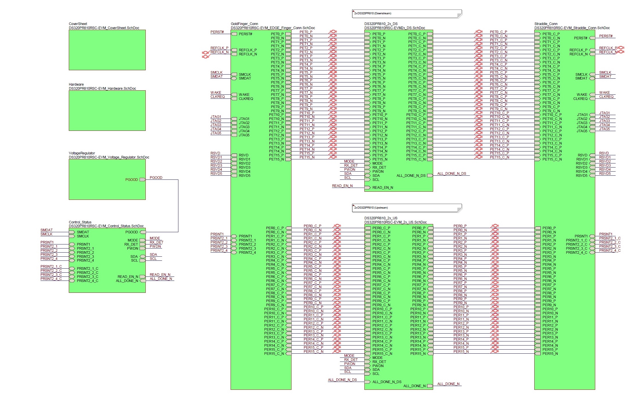 Figure 4-1 Top Level
Schematic Page
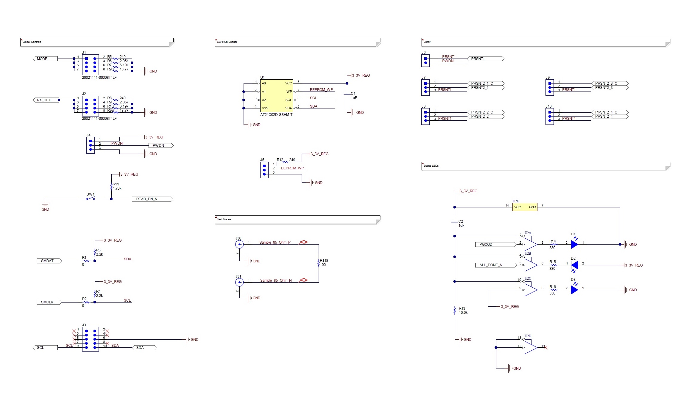 Figure 4-2 Control and Status Schematic Page
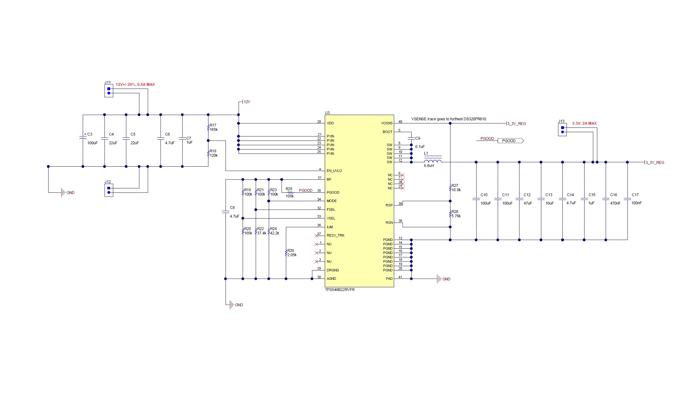 Figure 4-3 Voltage Regulator Schematic Page
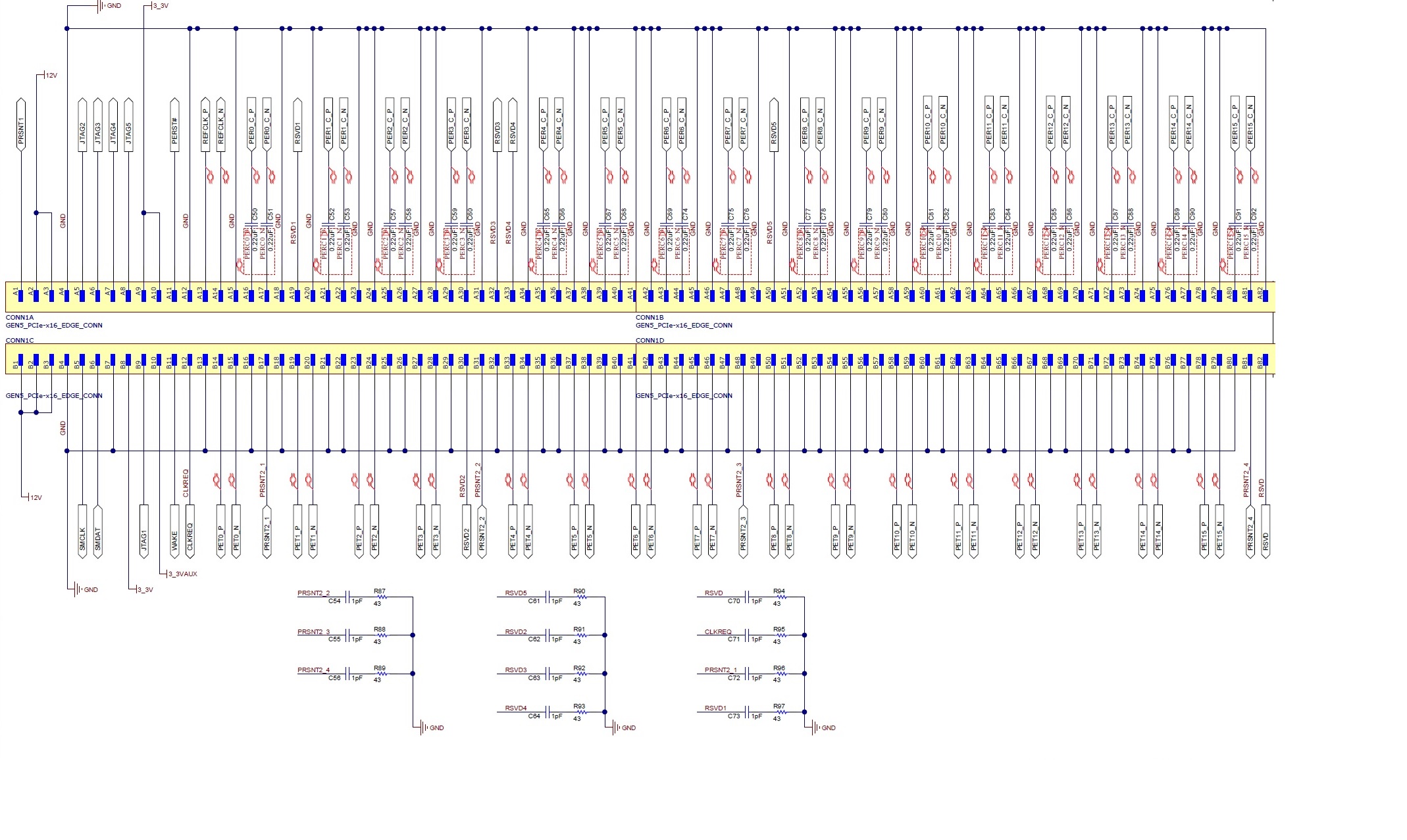 Figure 4-4 Gold Finger Connector Schematic Page
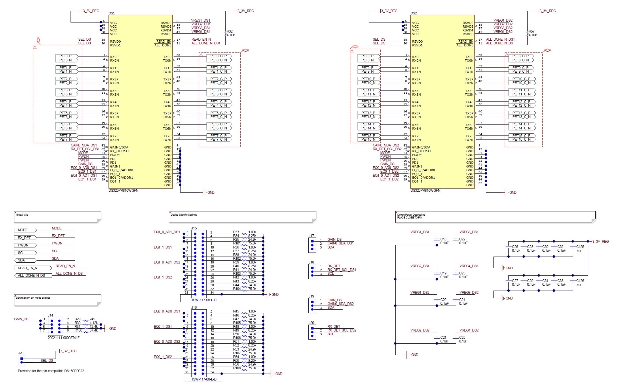 Figure 4-5 Downstream Devices Schematic Page
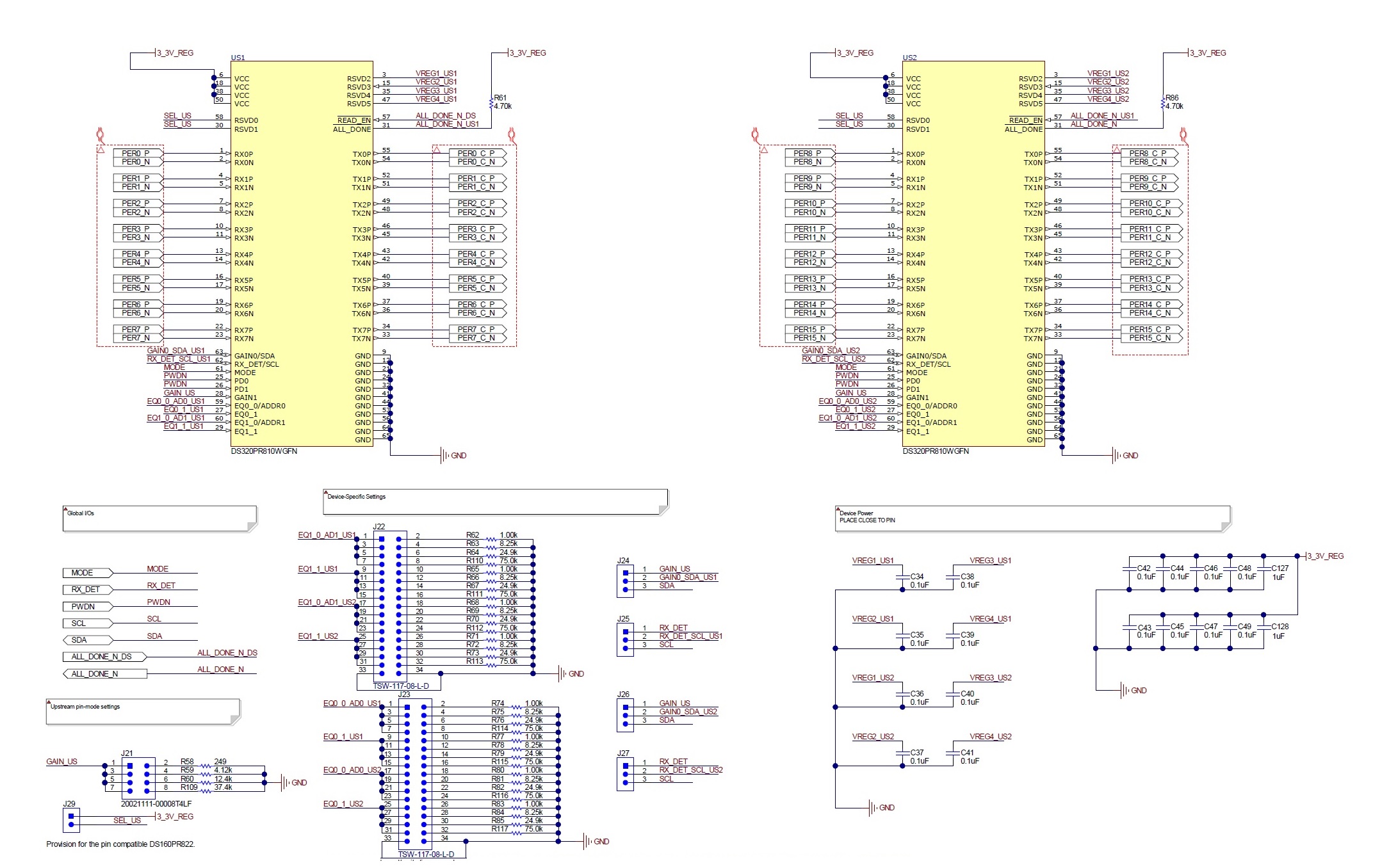 Figure 4-6 Upstream Devices Schematic Page
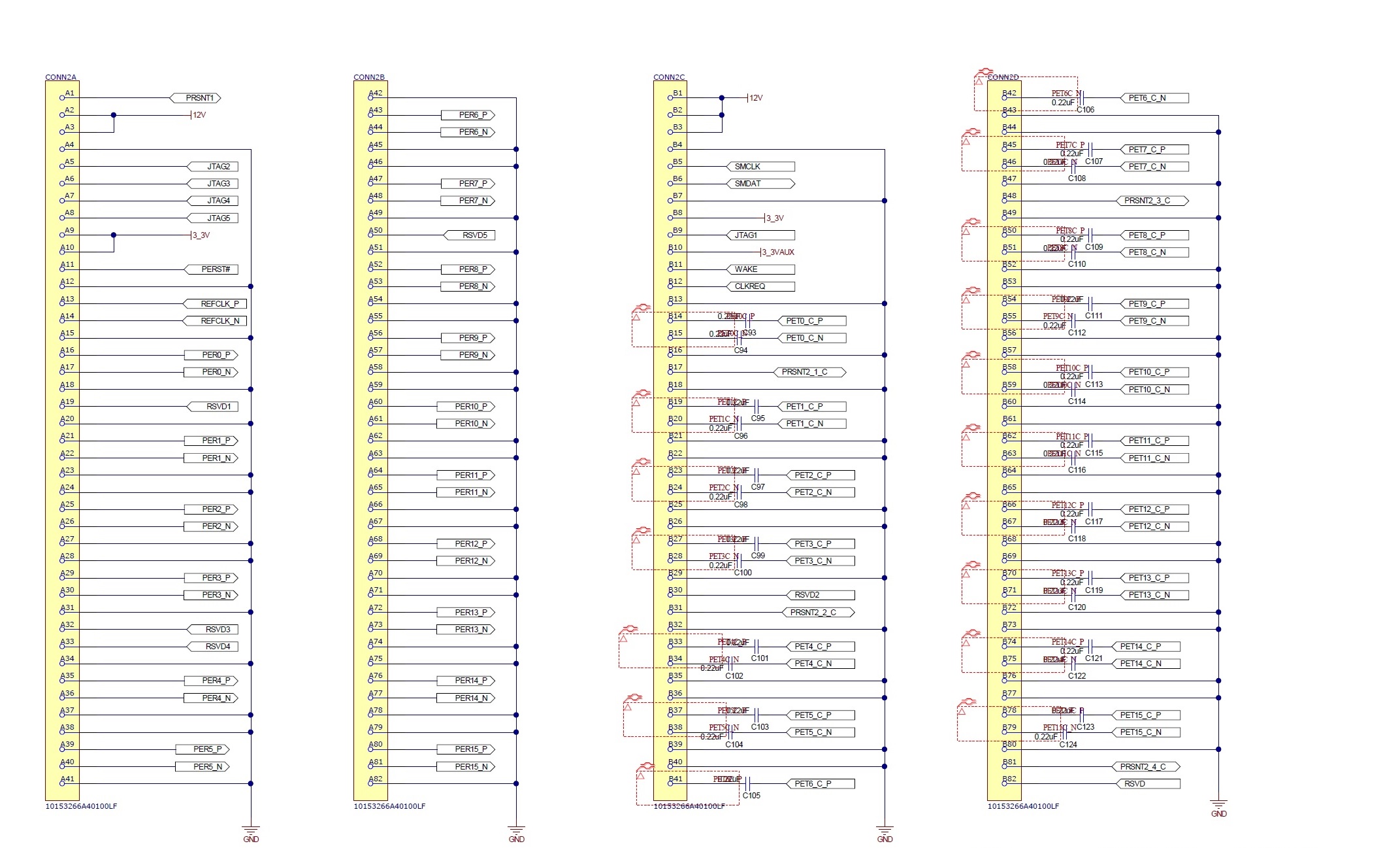 Figure 4-7 Straddle
Connector Schematic Page
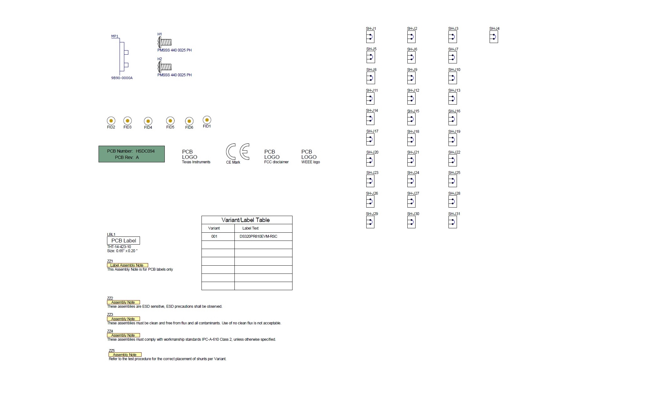 Figure 4-8 Hardware Page