SNLU346 May 2024 TUSB2E221
3.2 Board Layout
The TUSB2E221EVM was laid out with the following considerations:
- USB 2.0 signals impedance controlled 90Ω differential ± 5%.
- eUSB2 signals impedance controlled 45Ω signal ended ± 5%.
- USB 2.0 and eUSB2 signal pairs routed with matched trace lengths and minimal vias.
- All other signals to be impedance controlled 45Ω ± 10% or 50Ω ± 10%.
General information about the PCB is provided below:
- Finished board thickness: .062 ± 10% – necessary for socket
- Copper weight: 1oz start internal, 1/2 oz start external
- Laminate material: FR4 Polyclad 370 or equivalent
A four layer stack-up was used for the TUSB2E221EVM.
Drill notes on board stack up to account for the small BGA breakout:
- 1. L1 – L2 (laser drill) used for small pitch BGA break out.
- 2. L2 – L3 (mechanical drill) completes the small pitch BGA breakout.
- 3. L3 – L4 (laser drill) for VPP.
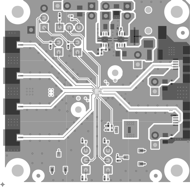
 Figure 3-2 TUSB2E221EVM PCB Top Layer
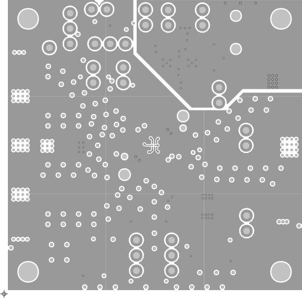
 Figure 3-4 TUSB2E221EVM PCB Layer 3 (Power Plane)
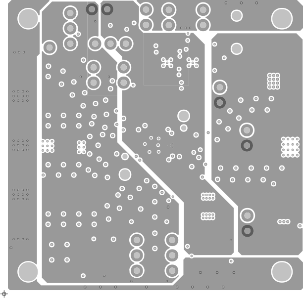
 Figure 3-3 TUSB2E221EVM PCB Layer 2 (Ground Plane)
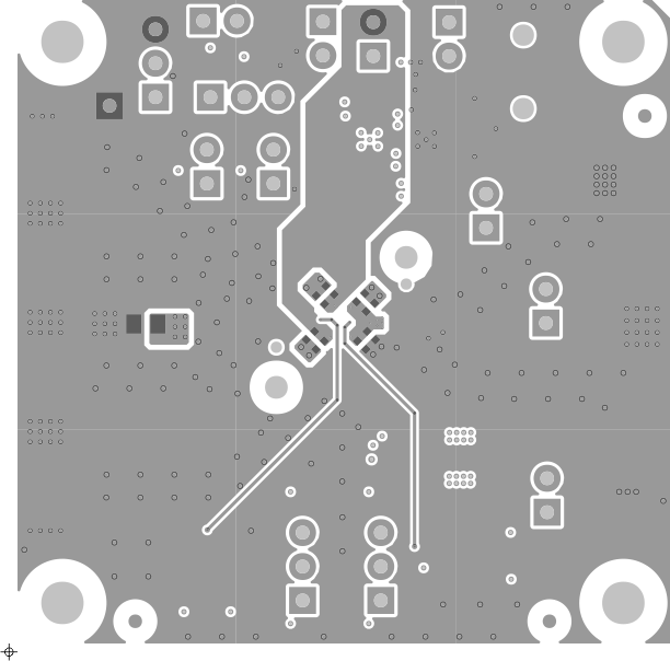
 Figure 3-5 TUSB2E221EVM Layer 4 (Bottom)