SNOA475F October 2016 – September 2020 LMV791
- Trademarks
- 1Introduction
-
2What Parameters Should Be Tested?
- 2.1 Open-Loop Gain (AOL) and Phase Margin
- 2.2 Slew Rate
- 2.3 Common-Mode Rejection Ratio (CMRR) and Power Supply Rejection Ratio (PSRR)
- 2.4 Open-Loop Output Impedance (Zo)
- 2.5 Voltage Noise (en)
- 2.6 Current Noise (in)
- 2.7 Input Offset Voltage (VOS), Input Bias Current (Ib), and Quiescent Current (IQ)
- 2.8 Output Voltage Versus Output Current (Claw Curve)
- 2.9 Overload Recovery Time (tOR)
- 2.10 Common-mode Input Capacitance (CCM) and Common-mode Differential Capacitance (CDIFF)
- 2.11 Overshoot and Transient Response
- 2.12 Common-Mode Voltage Range (CMVR)
- 3Conclusion
- Revision History
2.5 Voltage Noise (en)
Noise is simply an unwanted signal, usually random in nature, that when combined with the desired signal results in error. There are two parts to a voltage noise density curve, the 1/f noise (flicker noise, pink noise, low frequency noise, or excess noise) and the broadband noise (white noise, Johnson noise, thermal noise, or resistor noise). The 1/f noise happens at very low frequencies whereas the broadband noise is across all frequencies. Having a lower 1/f noise is desirable, since 1/f noise can become very large at lower frequencies.
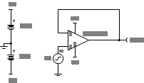
The op amp's voltage noise is usually given in units of nanovolts per square root hertz (nV/√Hz). The reason for such a complex unit is because the noise of a circuit is dependent on its bandwidth. Noise calculations involve integrating the behavior of noise sources over a specific frequency range, and the unit of nanovolts per root hertz simplifies to the RMS voltage after calculating the square root of the integral. Figure 2-15 below shows the Voltage Noise Test Circuit. To learn more about voltage noise (en), please refer to Texas Instruments Precision Labs video series on noise.
 Figure 2-15 Voltage Noise (en)
Test Circuit
Figure 2-15 Voltage Noise (en)
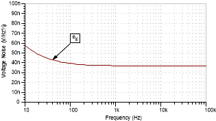
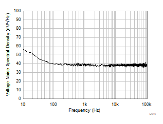
Test CircuitThis circuit places the op amp in a unity gain buffer configuration, with the input voltage source connected to the non-inverting input. This test setup generates a buffered copy of the input voltage noise at the op amp's output terminal for easy measurement. It's good practice to verify that the op amp is operating in the linear region by running a DC operating point test. Make sure to match the specified data sheet conditions for the power supply voltage, input common-mode voltage and load resistance (RL) if any. To measure en, run a noise analysis over the desired frequency range and plot the results at the output node with respect to the input source. Figure 2-16 shows the simulated voltage noise results for LM358B and is confirmed by Figure 2-17 that shows the data sheet graph of voltage noise for LM358B. For a more complete simulation test analysis, please refer to the following EDN article, authored by Ian Williams. This circuit may be simulated by downloading the AN1516 Test Circuits in either TINA-TI™ or PSpice® for TI.
 Figure 2-16 Simulated Voltage Noise
(en) for LM358B
 Figure 2-17 Data sheet Graph of
Voltage Noise (en) for LM358B