SNOAA69 April 2021 LM36922 , LM36923 , LM3697
4 LM369xx PCB Layout Tips
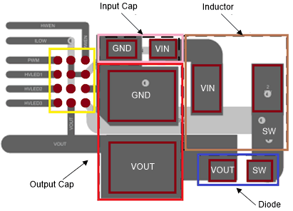
Good PCB layout ensures superb performance. Figure 4-1 shows an effective layout using the LM3697 device.

Figure 4-1 LM3697 PCB Layout
- Place the CIN and COUT capacitors and the Schottky diode close to the LM3697, the power trace should be short and wide to decrease power loss on the PCB trace.
- Place the L inductor close to the LM3697.
- The width of the power trace between the inductor and LM3697 should be 10 mil or more to decrease the noise and power dissipation on the power trace, and meanwhile optimize EMI performance.
- The width of the SW trace must be more than 10 mil especially for the inner layer or bottom layer, for the quantity of vias connected to the inductor is no less than 3 to decrease dv/dt and improve EMI performance.
- The width of the power trace between CIN and COUT and the LM3697 should be more than 10 mil to decrease the noise and power dissipation on the power trace, meanwhile this optimizes EMI performance.
- The GND pin should be connected to main ground plane (Brown color layer) directly to get better thermal sink and better EMI performance.