SNOSCY4E March 2015 – October 2018 LMG5200
PRODUCTION DATA.
- 1 Features
- 2 Applications
- 3 Description
- 4 Revision History
- 5 Pin Configuration and Functions
- 6 Specifications
- 7 Parameter Measurement Information
- 8 Detailed Description
- 9 Application and Implementation
- 10Power Supply Recommendations
- 11Layout
- 12Device and Documentation Support
- 13Mechanical, Packaging, and Orderable Information
11.2 Layout Examples
Placements shown in Figure 14 and in the cross section of Figure 15 show the suggested placement of the device with respect to sensitive passive components, such as VIN, bootstrap capacitors (HS and HB) and VSS capacitors. Use appropriate spacing in the layout to reduce creepage and maintain clearance requirements in accordance with the application pollution level. Inner layers if present can be more closely spaced due to negligible pollution.
The layout must be designed to minimize the capacitance at the SW node. Use as small an area of copper as possible to connect the device SW pin to the inductor, or transformer, or other output load. Furthermore, ensure that the ground plane or any other copper plane has a cutout so that there is no overlap with the SW node, as this would effectively form a capacitor on the printed circuit board. Additional capacitance on this node reduces the advantages of the advanced packaging approach of the LMG5200 and may result in reduced performance. Figure 16, Figure 17, Figure 18, and Figure 19 show an example of how to design for minimal SW node capacitance on a four-layer board. In these figures, U1 is the LMG5200 device.
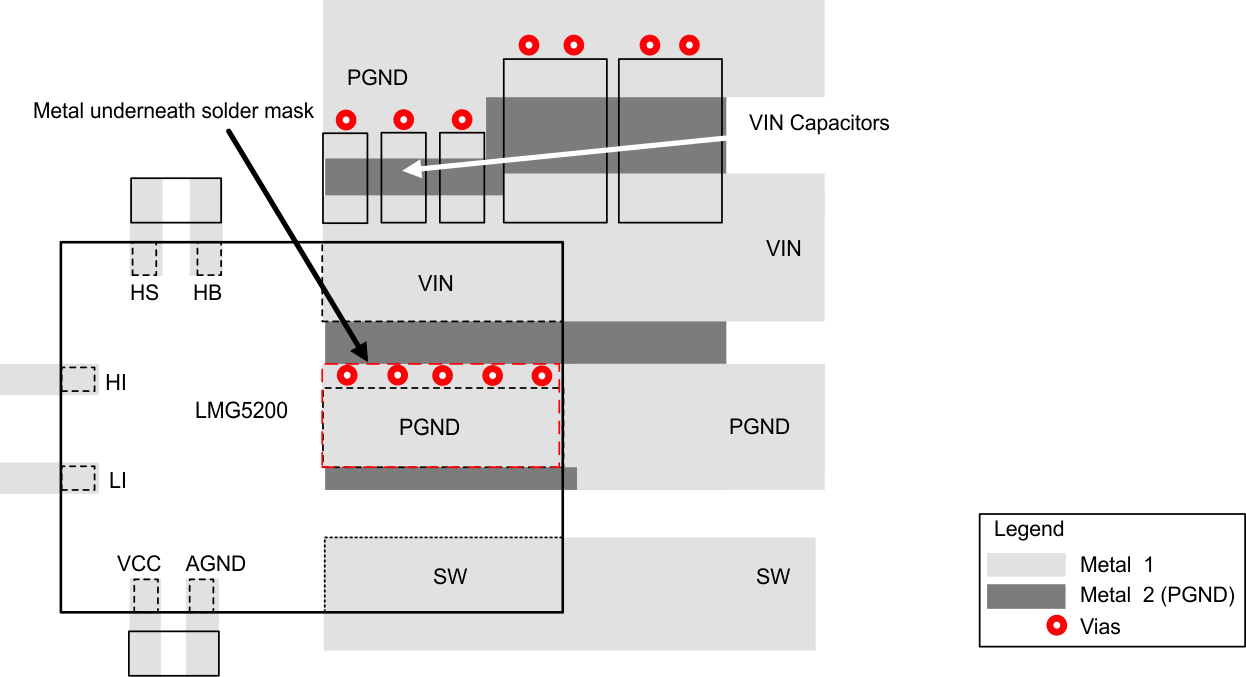 Figure 14. External Component Placement (Single Layer)
 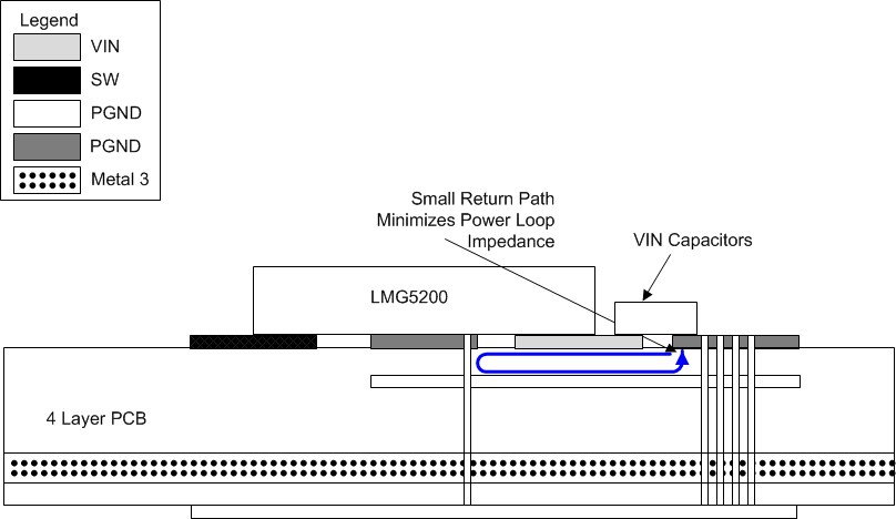 Figure 15. Four-Layer Board Cross Section With Return Path Directly Underneath for Power Loop
 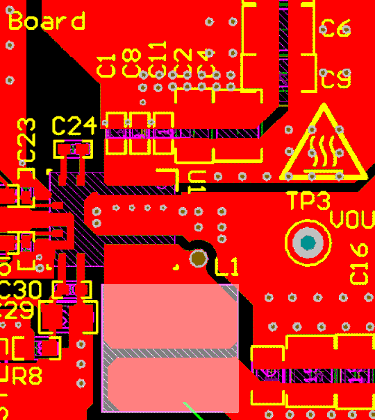 Figure 16. Top Layer
 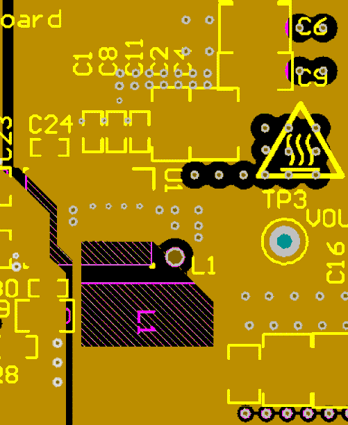 Figure 18. Middle Layer
 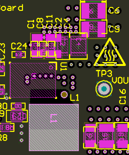 Figure 17. Ground Plane
 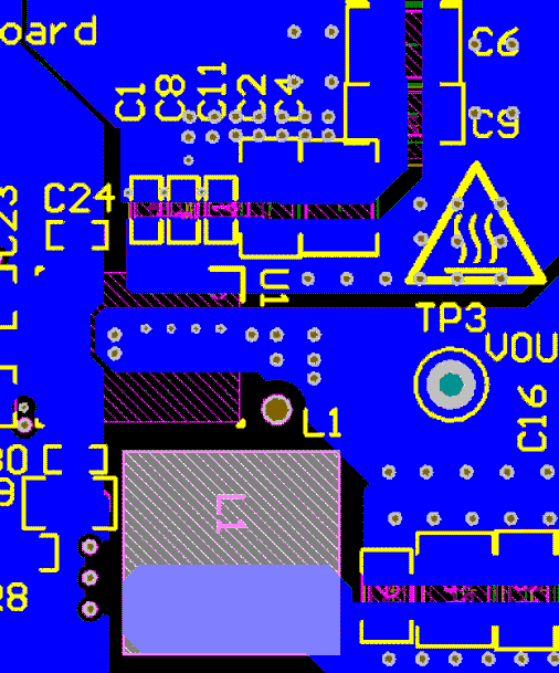 Figure 19. Bottom Layer
 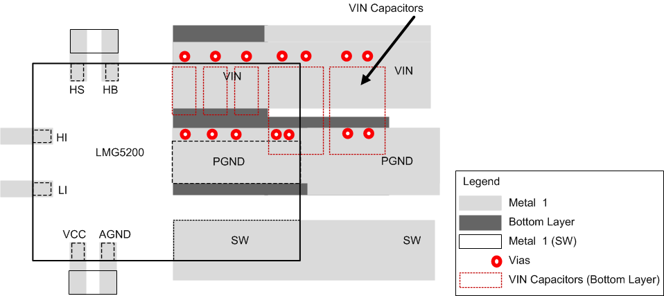 Figure 20. External Component Placement (Double Layer PCB)
 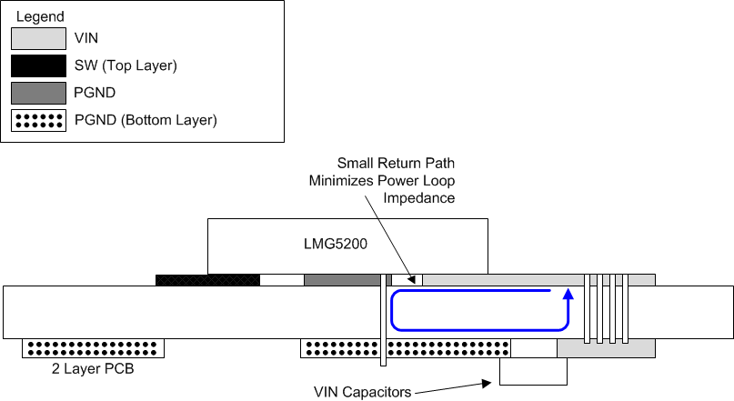 Figure 21. Two-Layer Board Cross Section With Return Path
 Two-layer boards are not recommended for use with LMG5200 device due to the larger power loop inductance. However, if design considerations allow only two board layers, place the input decoupling capacitors immediately behind the device on the back-side of the board to minimize loop inductance. Figure 20 and Figure 21 show a layout example for two-layer boards.