SNVA057D August 2002 – February 2022 LM2727 , LM2737
7 PCB Layout
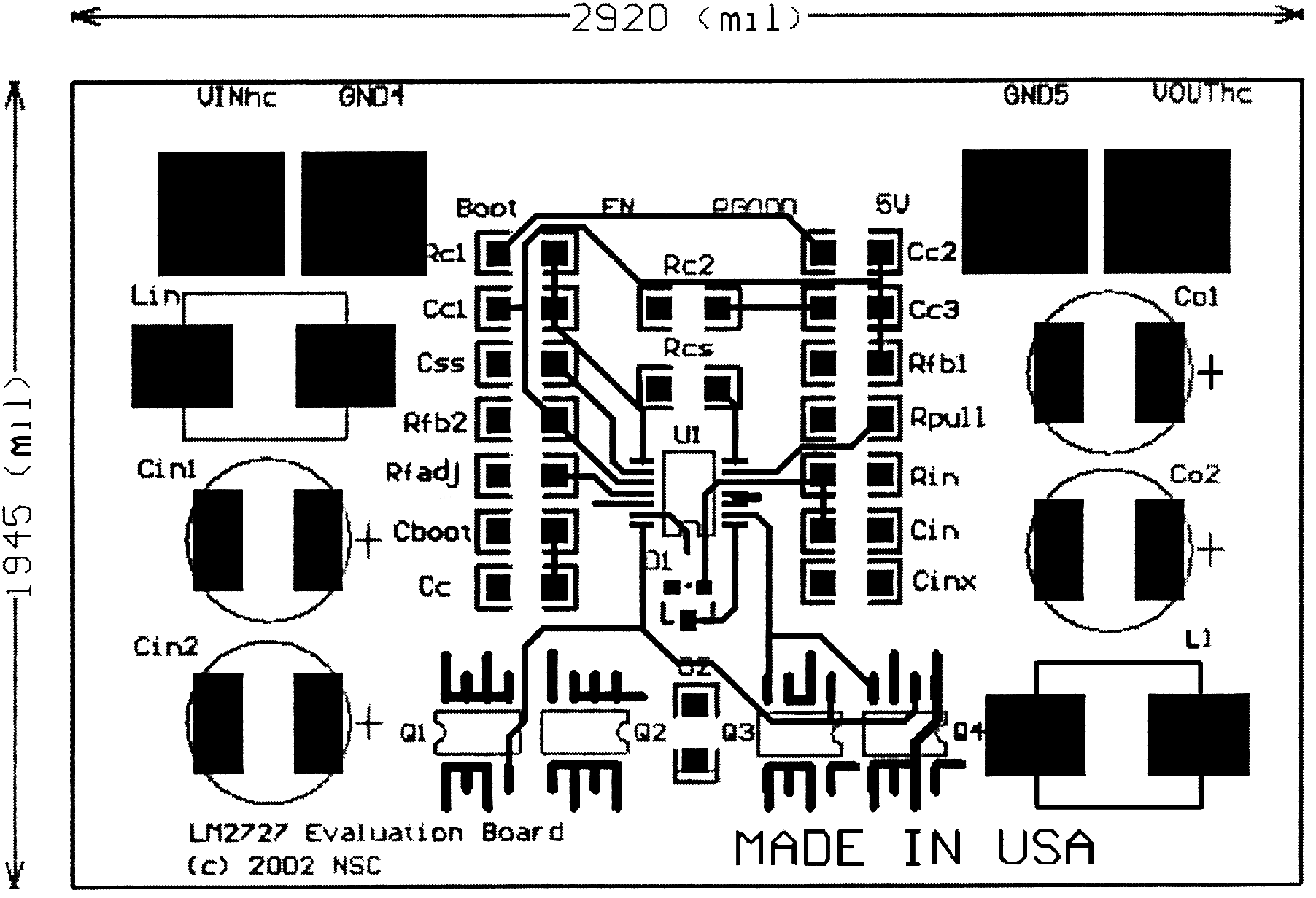
 Figure 7-1 PCB Top Layer and Top
Overlay
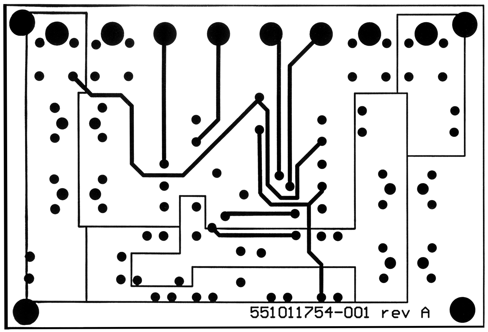
 Figure 7-2 PCB Bottom Layer and Internal
Power Plane
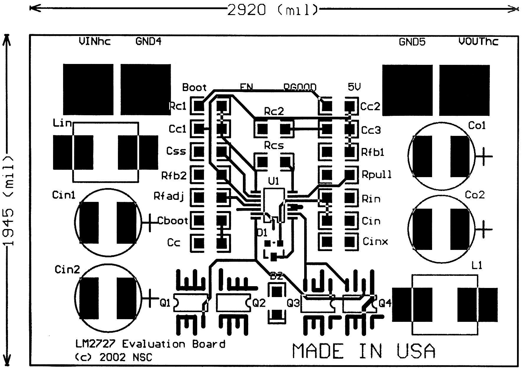
 Figure 7-3 PCB Overall