SNVS256E
November 2003 – October 2024
LP3943
PRODUCTION DATA
1
1
Features
2
Applications
3
Description
4
Pin Configuration and Functions
Pin Functions
5
Specifications
5.1
Absolute Maximum Ratings
5.2
ESD Ratings
5.3
Recommended Operating Conditions
5.4
Thermal Information
5.5
Electrical Characteristics
5.6
I2C Interface (SCL and SDA Pins) Timing Requirements
5.7
Typical Characteristic
6
Detailed Description
6.1
Overview
6.2
Functional Block Diagram
6.3
Feature Description
6.4
Device Functional Modes
6.5
Programming
6.5.1
I2C Data Validity
6.5.2
I2C START and STOP Conditions
6.5.3
Transferring Data
6.5.4
Auto Increment
6.6
Register Maps
6.6.1
Binary Format for Input Registers (Read-only)—Address 0x00 and 0x01
6.6.2
Binary Format for Frequency Prescaler and PWM Registers — Address 0x02 to 0x05
6.6.3
Binary Format for Selector Registers — Address 0x06 to 0x09
Application and Implementation
7.1
Application Information
7.2
Typical Application
7.2.1
Design Requirements
7.2.2
Detailed Design Procedure
7.2.2.1
Reducing IQ When LEDs are OFF
7.2.3
Application Curve
7.3
System Examples
7.4
Power Supply Recommendations
7.5
Layout
7.5.1
Layout Guidelines
7.5.2
Layout Example
7
Device and Documentation Support
7.1
Receiving Notification of Documentation Updates
7.2
Community Resources
7.3
Trademarks
8
Revision History
Mechanical, Packaging, and Orderable Information
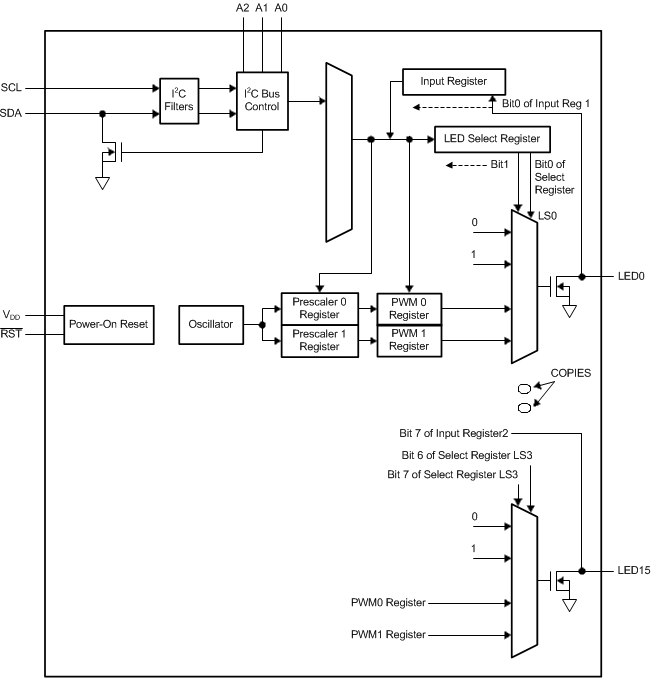
6.2
Functional Block Diagram