SNVS256E November   2003  – October 2024 LP3943

PRODUCTION DATA  

  1.   1
  2. 1Features
  3. 2Applications
  4. 3Description
  5. 4Pin Configuration and Functions
    1.     Pin Functions
  6. 5Specifications
    1. 5.1 Absolute Maximum Ratings
    2. 5.2 ESD Ratings
    3. 5.3 Recommended Operating Conditions
    4. 5.4 Thermal Information
    5. 5.5 Electrical Characteristics
    6. 5.6 I2C Interface (SCL and SDA Pins) Timing Requirements
    7. 5.7 Typical Characteristic
  7. 6Detailed Description
    1. 6.1 Overview
    2. 6.2 Functional Block Diagram
    3. 6.3 Feature Description
    4. 6.4 Device Functional Modes
    5. 6.5 Programming
      1. 6.5.1 I2C Data Validity
      2. 6.5.2 I2C START and STOP Conditions
      3. 6.5.3 Transferring Data
      4. 6.5.4 Auto Increment
    6. 6.6 Register Maps
      1. 6.6.1 Binary Format for Input Registers (Read-only)—Address 0x00 and 0x01
      2. 6.6.2 Binary Format for Frequency Prescaler and PWM Registers — Address 0x02 to 0x05
      3. 6.6.3 Binary Format for Selector Registers — Address 0x06 to 0x09
  8.   Application and Implementation
    1. 7.1 Application Information
    2. 7.2 Typical Application
      1. 7.2.1 Design Requirements
      2. 7.2.2 Detailed Design Procedure
        1. 7.2.2.1 Reducing IQ When LEDs are OFF
      3. 7.2.3 Application Curve
    3. 7.3 System Examples
    4. 7.4 Power Supply Recommendations
    5. 7.5 Layout
      1. 7.5.1 Layout Guidelines
      2. 7.5.2 Layout Example
  9. 7Device and Documentation Support
    1. 7.1 Receiving Notification of Documentation Updates
    2. 7.2 Community Resources
    3. 7.3 Trademarks
  10. 8Revision History
  11.   Mechanical, Packaging, and Orderable Information

Transferring Data

Every byte put on the SDA line must be eight bits long with the most significant bit (MSB) being transferred first. The number of bytes that can be transmitted per transfer is unrestricted. Each byte of data has to be followed by an acknowledge bit. The acknowledge related clock pulse is generated by the master. The transmitter releases the SDA line (HIGH) during the acknowledge clock pulse. The receiver must pull down the SDA line during the 9th clock pulse, signifying an acknowledge. A receiver which has been addressed must generate an acknowledge after each byte has been received.

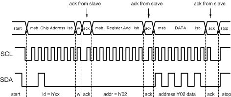
After the START condition, a chip address is sent by the I2C master. This address is seven bits long followed by an eighth bit which is a data direction bit (R/W). The LP3943 hardwires bits 7 to 4 and leaves bits 3 to 1 selectable, as shown in Figure 6-3. For the eighth bit, a 0 indicates a WRITE and a 1 indicates a READ. The LP3943 supports only a WRITE during chip addressing. The second byte selects the register to which the data is written. The third byte contains data to write to the selected register.

LP3943 Chip Address ByteFigure 6-3 Chip Address Byte
LP3943 LP3943 Register Write
w = write (SDA = 0) r = read (SDA = 1) ack = acknowledge (SDA pulled LOW by either master or slave) rs = repeated start xx = 60 to 67
Figure 6-4 LP3943 Register Write

However, if a READ function is to be accomplished, a WRITE function must precede the READ function, as shown in Figure 6-5.

LP3943 LP3943 Register Read
w = write (SDA = “0”) r = read (SDA = “1”) ack = acknowledge (SDA pulled LOW by either master or slave) rs = repeated start xx = 60 to 67
Figure 6-5 LP3943 Register Read