SNVSAA7B December   2015  – July 2021 LM53625-Q1 , LM53635-Q1

PRODUCTION DATA  

  1. Features
  2. Applications
  3. Description
  4. Revision History
  5. Device Comparison
  6. Pin Configuration and Functions
  7. Specifications
    1. 7.1 Absolute Maximum Ratings
    2. 7.2 ESD Ratings
    3. 7.3 Recommended Operating Conditions
    4. 7.4 Thermal Information
    5. 7.5 Electrical Characteristics
    6. 7.6 System Characteristics
    7. 7.7 Timing Characteristics
    8. 7.8 Typical Characteristics
  8. Detailed Description
    1. 8.1 Overview
    2. 8.2 Functional Block Diagram
      1. 8.2.1 Control Scheme
    3. 8.3 Feature Description
      1. 8.3.1 RESET Flag Output
      2. 8.3.2 Enable and Start-Up
      3. 8.3.3 Soft-Start Function
      4. 8.3.4 Current Limit
      5. 8.3.5 Hiccup Mode
      6. 8.3.6 Synchronizing Input
      7. 8.3.7 Undervoltage Lockout (UVLO) and Thermal Shutdown (TSD)
      8. 8.3.8 Input Supply Current
    4. 8.4 Device Functional Modes
      1. 8.4.1 AUTO Mode
      2. 8.4.2 FPWM Mode
      3. 8.4.3 Dropout
      4. 8.4.4 Input Voltage Frequency Foldback
    5. 8.5 Spread-Spectrum Operation
  9. Application and Implementation
    1. 9.1 Application Information
    2. 9.2 Typical Applications
      1. 9.2.1 General Application
        1. 9.2.1.1 Design Requirements
        2. 9.2.1.2 Detailed Design Procedure
          1. 9.2.1.2.1 External Components Selection
            1. 9.2.1.2.1.1 Input Capacitors
              1. 9.2.1.2.1.1.1 Input Capacitor Selection
            2. 9.2.1.2.1.2 Output Inductors and Capacitors Selection
              1. 9.2.1.2.1.2.1 Inductor Selection
              2. 9.2.1.2.1.2.2 Output Capacitor Selection
          2. 9.2.1.2.2 Setting the Output Voltage
            1. 9.2.1.2.2.1 FB for Adjustable Versions
          3. 9.2.1.2.3 VCC
          4. 9.2.1.2.4 BIAS
          5. 9.2.1.2.5 CBOOT
          6. 9.2.1.2.6 Maximum Ambient Temperature
        3. 9.2.1.3 Application Curves
      2. 9.2.2 Fixed 5-V Output for USB-Type Applications
        1. 9.2.2.1 Design Requirements
        2. 9.2.2.2 Detailed Design Procedure
        3. 9.2.2.3 Application Curves
      3. 9.2.3 Fixed 3.3-V Output
        1. 9.2.3.1 Design Requirements
        2. 9.2.3.2 Detailed Design Procedure
        3. 9.2.3.3 Application Curves
      4. 9.2.4 Adjustable Output
        1. 9.2.4.1 Design Requirements
        2. 9.2.4.2 Detailed Design Procedure
        3. 9.2.4.3 Application Curves
    3. 9.3 What to Do and What Not to Do
  10. 10Power Supply Recommendations
  11. 11Layout
    1. 11.1 Layout Guidelines
    2. 11.2 Layout Example
  12. 12Device and Documentation Support
    1. 12.1 Device Support
      1. 12.1.1 Third-Party Products Disclaimer
    2. 12.2 Documentation Support
      1. 12.2.1 Related Documentation
    3. 12.3 Receiving Notification of Documentation Updates
    4. 12.4 Support Resources
    5. 12.5 Trademarks
    6. 12.6 Electrostatic Discharge Caution
    7. 12.7 Glossary
  13. 13Mechanical, Packaging, and Orderable Information

Dropout

One of the parameters that influences the dropout performance of a buck regulator is the minimum off time. As the input voltage is reduced, to near the output voltage, the off time of the high-side switch starts to approach the minimum value (see Section 7.5). Beyond this point the switching may become erratic and/or the output voltage falls out of regulation. To avoid this problem, the LM53625/35-Q1 automatically reduces the switching frequency to increase the effective duty cycle. This results in two specifications regarding dropout voltage, as shown in Section 7.6. One specification indicates when the switching frequency drops to 1.85 MHz; avoiding the A.M. radio band. The other specification indicates when the output voltage has fallen to 3% of nominal. See the Section 9.2.2.3 for typical dropout values. The overall dropout characteristic for the 5-V option can be seen in Figure 8-11 and Figure 8-12. The SYNC input is ignored during frequency foldback in dropout. Additional dropout information is discussed in for 5-V output (Section 9.2.2.3 and for 3.3 V output (Section 9.2.3.3).
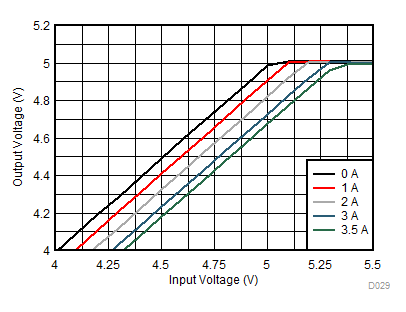
GUID-068B8178-D0B2-42CA-8950-F91CA527AB04-low.gifFigure 8-11 Overall Dropout Characteristics (VOUT = 5 V)
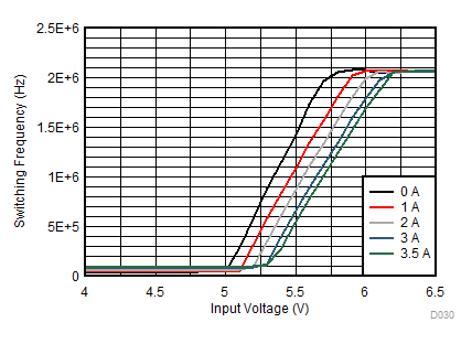
GUID-88FD6A57-85B6-4AF9-8A40-6DA9B4D48F89-low.gifFigure 8-12 Frequency Dropout Characteristics (VOUT = 5 V)