SNVSB06D July 2018 – May 2020 LM5180
PRODUCTION DATA.
- 1 Features
- 2 Applications
- 3 Description
- 4 Revision History
- 5 Description (continued)
- 6 Pin Configuration and Functions
- 7 Specifications
-
8 Detailed Description
- 8.1 Overview
- 8.2 Functional Block Diagram
- 8.3
Feature Description
- 8.3.1 Integrated Power MOSFET
- 8.3.2 PSR Flyback Modes of Operation
- 8.3.3 Setting the Output Voltage
- 8.3.4 Control Loop Error Amplifier
- 8.3.5 Precision Enable
- 8.3.6 Configurable Soft Start
- 8.3.7 External Bias Supply
- 8.3.8 Minimum On-Time and Off-Time
- 8.3.9 Overcurrent Protection
- 8.3.10 Thermal Shutdown
- 8.4 Device Functional Modes
-
9 Application and Implementation
- 9.1 Application Information
- 9.2
Typical Applications
- 9.2.1
Design 1: Wide VIN, Low IQ PSR Flyback Converter Rated at 5 V, 1 A
- 9.2.1.1 Design Requirements
- 9.2.1.2
Detailed Design Procedure
- 9.2.1.2.1 Custom Design With WEBENCH® Tools
- 9.2.1.2.2 Custom Design With Excel Quickstart Tool
- 9.2.1.2.3 Flyback Transformer – T1
- 9.2.1.2.4 Flyback Diode – DFLY
- 9.2.1.2.5 Zener Clamp Circuit – DF, DCLAMP
- 9.2.1.2.6 Output Capacitor – COUT
- 9.2.1.2.7 Input Capacitor – CIN
- 9.2.1.2.8 Feedback Resistor – RFB
- 9.2.1.2.9 Thermal Compensation Resistor – RTC
- 9.2.1.2.10 UVLO Resistors – RUV1, RUV2
- 9.2.1.2.11 Soft-Start Capacitor – CSS
- 9.2.1.3 Application Curves
- 9.2.2 Design 2: PSR Flyback Converter With Dual Outputs of 15 V and –7.7 V at 200 mA
- 9.2.3 Design 3: PSR Flyback Converter With Stacked Dual Outputs of 24 V and 5 V
- 9.2.1
Design 1: Wide VIN, Low IQ PSR Flyback Converter Rated at 5 V, 1 A
- 10Power Supply Recommendations
- 11Layout
- 12Device and Documentation Support
- 13Mechanical, Packaging, and Orderable Information
8.3.1 Integrated Power MOSFET
The LM5180 is a flyback dc/dc converter with integrated 100-V, 1.5-A N-channel power MOSFET. During the MOSFET on-time, the transformer primary current increases from zero with slope VIN / LMAG (where LMAG is the transformer primary-referred magnetizing inductance) while the output capacitor supplies the load current. When the high-side MOSFET is turned off by the control logic, the SW voltage VSW swings up to approximately VIN + (NPS × VOUT), where NPS = NP/NS is the primary-to-secondary turns ratio of the transformer. The magnetizing current flows in the secondary side through the flyback diode, charging the output capacitor and supplying current to the load. Duty cycle D is defined as tON / tSW, where tON is the MOSFET conduction time and tSW is the switching period.
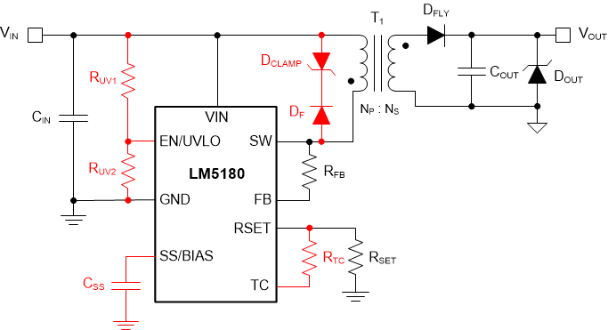
Figure 19 shows a typical schematic of the LM5180 PSR flyback circuit. Components denoted in red are optional depending on the application requirements.
 Figure 19. LM5180 Flyback Converter Schematic (Optional Components in Red)