SNVSBU4E June 2022 – August 2024 LM5177
PRODUCTION DATA
- 1
- 1 Features
- 2 Applications
- 3 Description
- 4 Pin Configuration and Functions
- 5 Specifications
- 6 Parameter Measurement Information
-
7 Detailed Description
- 7.1 Overview
- 7.2 Functional Block Diagram
- 7.3
Feature Description
- 7.3.1 Power-On Reset (POR System)
- 7.3.2 Buck-Boost Control Scheme
- 7.3.3 Power Save Mode
- 7.3.4 Supply Voltage Selection – VMAX Switch
- 7.3.5 Enable and Undervoltage Lockout
- 7.3.6 Oscillator Frequency Selection
- 7.3.7 Frequency Synchronization
- 7.3.8 Voltage Regulation Loop
- 7.3.9 Output Voltage Tracking
- 7.3.10 Slope Compensation
- 7.3.11 Configurable Soft Start
- 7.3.12 Peak Current Sensor
- 7.3.13 Current Monitoring and Current Limit Control Loop
- 7.3.14 Short Circuit - Hiccup Protection
- 7.3.15 nFLT Pin and Protections
- 7.3.16 Device Configuration Pin
- 7.3.17 Dual Random Spread Spectrum – DRSS
- 7.3.18 Gate Driver
- 7.4 Device Functional Modes
-
8 Application and Implementation
- 8.1 Application Information
- 8.2
Typical Application
- 8.2.1 Design Requirements
- 8.2.2
Detailed Design Procedure
- 8.2.2.1 Custom Design with WEBENCH Tools
- 8.2.2.2 Frequency
- 8.2.2.3 Feedback Divider
- 8.2.2.4 Inductor and Current Sense Resistor Selection
- 8.2.2.5 Slope Compensation
- 8.2.2.6 Output Capacitor
- 8.2.2.7 Input Capacitor
- 8.2.2.8 UVLO Divider
- 8.2.2.9 Soft-Start Capacitor
- 8.2.2.10 MOSFETs QH1 and QL1
- 8.2.2.11 MOSFETs QH2 and QL2
- 8.2.2.12 Frequency Compensation
- 8.2.2.13 External Component Selection
- 8.2.3 Application Curves
- 8.3 System Examples
- 9 Power Supply Recommendations
- 10Layout
- 11Device and Documentation Support
- 12Revision History
- 13Mechanical, Packaging, and Orderable Information
8.3.1 Bi-Directional Power Backup
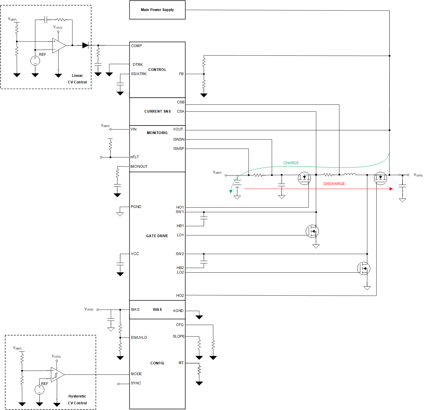
The precise reverse current limit of the device enables the LM5177 to charge a storage element on the input of the power stage. Once the integrated average current limitation circuit of the LM5177 is enabled on the input, the third regulation loop maintains a constant current operation to charge the storage on the input for example a battery or super-capacitor array. The end of charge voltage for the input can be regulated by a simple hysteric regulation approach or by using a linear approach with an external operational amplifier as well as an equivalent digital regulation scheme.
Once the system power supply is interrupted or has a malfunction the LM5177 imitatively supplies the connected system load as soon the selected backup voltage threshold triggers. The seamless transition is maintained by the buck-boost voltage control loop, which stays in regulation during charging and ensures a minimum voltage drop for the connected system during backup.
Benefits:
- Seamless and automatic transition from main system supply to the power backup
- Combination of energy storage charging control and backup regulator with a single chip solution
- Single inductor solution, that is one power stage for charging and backup operation
- Constant current constant voltage operation possible to realize with
- Adjustable on-the-fly transition voltage using the output feedback divider
- Scalable solution for multiple systems. Power levels are adjusted with the BOM. Topologies and architecture qualification maintains the same.

Figure 8-16 Simplified Schematic of a Bi-Directional Operation
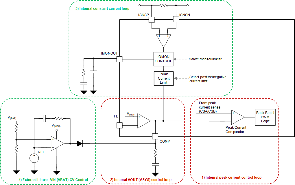
Below you find a overview for the control loop interacting together in the DC/DC Backup application. The central point for the interaction is the COMP pin which defines the peak current target for the underlying bi-directional peak current control loop
- Internal peak current loop. The control input signal from the COMP pin sets the bi-directional (positive and negative pack current) for the PWM logic.
- The internal output voltage loop is controlling the Vo or system voltage once the system supply voltage is not there anymore and Vo drops below the selected voltage by the FB-PIN
- The internal constant current loop limits and regulates the peak current in the selected direction. For most power backup cases the negative (charging) current is selected. By activating the constant current limit the peak current gets clamped and cannot reach his full value which enables a lower charging current that the forward discharging current as the forward direction don’t get limited if the negative direction of the constant current loop is selected.
- The input voltage (VBAT) constant voltage regulation can be added externally with a linear regulator in the COMP-pin. Once the battery voltage reaches the desired target voltage the regulator pulls up the peak current set-point and the charging operation stops.

Figure 8-17 Overview of the Control loops for DC/DC Backup application